Method of manufacturing liquid crystal device and liquid crystal device

一种液晶装置、制造方法的技术,应用在光学、仪器、非线性光学等方向,能够解决液晶单元难、偏振光板的光轴对位、对位及粘贴工序变多等问题

Inactive Publication Date: 2010-06-02
SEIKO EPSON CORP
View PDF3 Cites 13 Cited by
  • Summary
  • Abstract
  • Description
  • Claims
  • Application Information

AI Technical Summary

Problems solved by technology

[0007] However, in the method described in the above-mentioned Patent Document 1, since the alignment mark and the outer shape of the polarizing plate are aligned, it is difficult to accurately align the polarizing plate with respect to the liquid crystal cell when the outer shape of the polarizing plate and the optical axis are misaligned. The problem of aligning the optical axis of the polarizing plate
In the method described in the above-mentioned patent document 2 and patent document 3, owing to the optical axis of the main polarizer is a reference, the alignment direction of the liquid crystal cell and the optical axis of each polarizing plate are independently aligned and pasted, so there are the following The problem is that the number of alignment and bonding processes increases man-hours, and if there is a shift in the position of the main polarizer, the shift will be reflected in the alignment of the liquid crystal cell and the polarizer

Method used


Image

  • Method of manufacturing liquid crystal device and liquid crystal device
  • Method of manufacturing liquid crystal device and liquid crystal device
  • Method of manufacturing liquid crystal device and liquid crystal device

Examples


no. 1 approach

[0079]

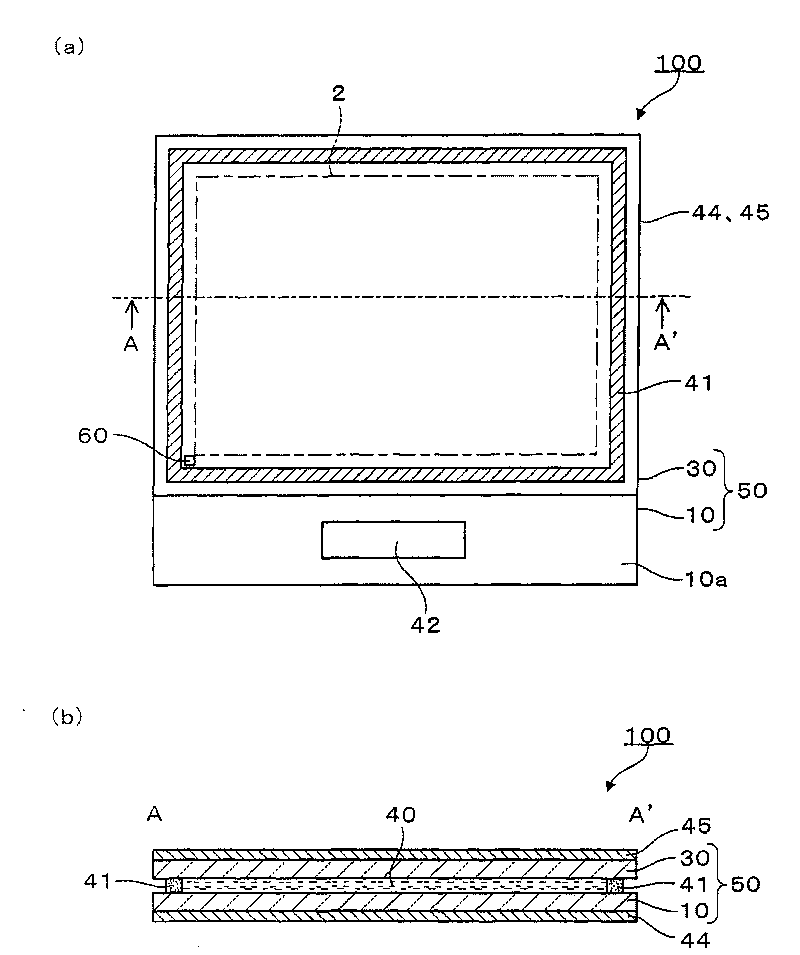
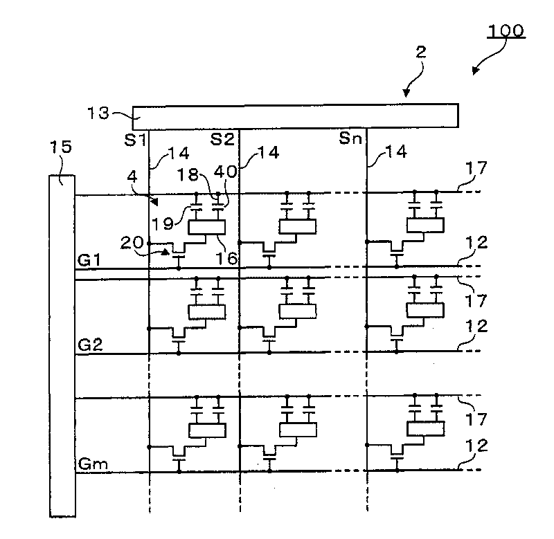
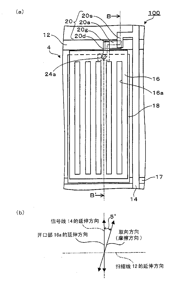
[0080] First, a liquid crystal device according to a first embodiment will be described with reference to the drawings. figure 1It is a figure showing the schematic structure of the liquid crystal device of 1st Embodiment. in particular, figure 1 (a) is a top view of a liquid crystal device, figure 1 (b) is along figure 1 A cross-sectional view of line A-A in (a). figure 2 It is an equivalent circuit diagram showing the electrical configuration of the liquid crystal device of the first embodiment. image 3 It is a figure explaining the structure of the pixel of the liquid crystal device of 1st Embodiment. in particular, image 3 (a) is a plan view showing the structure of a pixel viewed from the counter substrate side, image 3 (b) is a figure which shows the orientation direction of a liquid crystal cell. Figure 4 is along image 3 Section view of line B-B in (a). In addition, in image 3 In (a), illustration of the counter substrate is omitted.

[008...

no. 2 approach

[0149]

[0150] Next, a liquid crystal device according to a second embodiment will be described with reference to the drawings. Figure 11 It is a figure explaining the wire grid polarizer of 2nd Embodiment. In detail, Figure 11 (a) is a perspective view showing a schematic structure of a wire grid polarizer, Figure 11 (b) is a diagram showing optical design conditions.

[0151] The liquid crystal device of the second embodiment is different from the liquid crystal device of the first embodiment in that the directions of the transmission axis and the reflection axis of the wire grid polarizer are different, and the other structures are the same. The same reference numerals are assigned to the same constituent elements as those of the first embodiment, and description thereof will be omitted.

[0152] Such as Figure 11 As shown in (a), the wire grid polarizer 62 included in the liquid crystal device of the second embodiment includes a plurality of metal reflective fil...

no. 3 approach

[0163]

[0164] Next, a liquid crystal device and a manufacturing method thereof according to a third embodiment will be described with reference to the drawings. Figure 12 It is a plan view of the schematic structure of the liquid crystal device of 3rd Embodiment.

[0165] The liquid crystal device of the third embodiment differs from the liquid crystal device of the first embodiment in that the wire grid polarizer is disposed outside the region surrounded by the sealant 41 , and the structure is the same except for that. The same reference numerals are assigned to the same constituent elements as those of the first embodiment, and description thereof will be omitted.

[0166] exist Figure 12 In the example of the liquid crystal device 110 shown in (a), the wire grid polarizer 60 is disposed outside the area surrounded by the sealant 41 , that is, at a position not overlapping the liquid crystal layer 40 in plan view.

[0167] According to such a structure, even when th...


PUM


Abstract

The present invention provides a liquid crystal device manufacturing method for reducing the position deviation of an optical shaft of a liquid crystal unit and an optical shaft of a polarization optical plate and a liquid crystal device. The liquid crystal device manufacturing method includes: a working procedure for preparing the liquid crystal unit having a liquid crystal layer clamped between an element substrate and a contraposition substrate which are opposite to each other, at least one position arranged at the element substrate, and a wire grating polariscope with polarized light separating function; a first working procedure, under the state of contraposition of a polarized light plate with the outer side of the element substrate of the liquid crystal unit, at least one of the liquid crystal unit and the polarized light plate rotates in the contraposition surface, for detecting the intensity of light which passes through a region arranged with wire grating polariscope of the liquid crystal unit and the polarized light plate; and a second working procedure, according to the detection result of the intensity of the light, for determining the position relationship of the polarized light plate relative to the wire grating polariscope in the opposite surfaces, and adhering the polarized light plate on the element substrate of the liquid crystal unit.

Description

technical field [0001] The present invention relates to a method for manufacturing a liquid crystal device and a liquid crystal device. Background technique [0002] The liquid crystal device includes a liquid crystal cell in which a liquid crystal layer is sandwiched between a pair of opposed substrates, and a pair of polarizing plates arranged on both outer sides of the liquid crystal cell. Since the liquid crystal device performs display using polarized light, the alignment direction of the liquid crystal molecules in the liquid crystal layer and the optical axes of the pair of polarizing plates are set to form a predetermined positional relationship. Therefore, if the predetermined arrangement positions of the liquid crystal cell and the polarizing plate are shifted in the step of attaching the polarizing plate to the liquid crystal cell, desired optical characteristics (contrast, etc.) cannot be obtained, resulting in a decrease in display quality. [0003] Therefore, ...

Claims


Application Information

Patent Timeline
Patent Type & Authority Applications(China)
IPC IPC(8): G02F1/1335G02B5/30G02F1/1333
CPCG02F2001/133548G02F1/133528G02F2001/133638G02F1/133548G02F1/133638
Inventor 土屋丰关琢巳
Owner SEIKO EPSON CORP
Why Eureka
Try Eureka