Power device chip

A technology of power devices and chips, which is applied in the field of power device chips, and can solve problems such as weak current capabilities of power device chips

Inactive Publication Date: 2010-06-09
PEKING UNIV FOUNDER GRP CO LTD +1
View PDF0 Cites 7 Cited by
  • Summary
  • Abstract
  • Description
  • Claims
  • Application Information

AI Technical Summary

Problems solved by technology

[0003] In the prior art, whether the cells of the chip are regular hexagon...

Method used


Image

  • Power device chip
  • Power device chip
  • Power device chip

Examples


Embodiment Construction

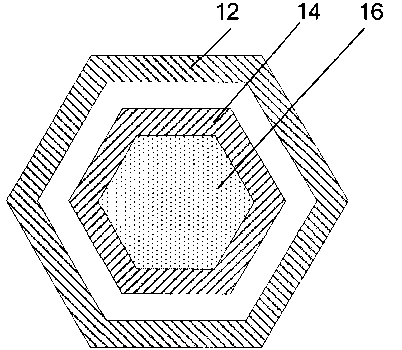
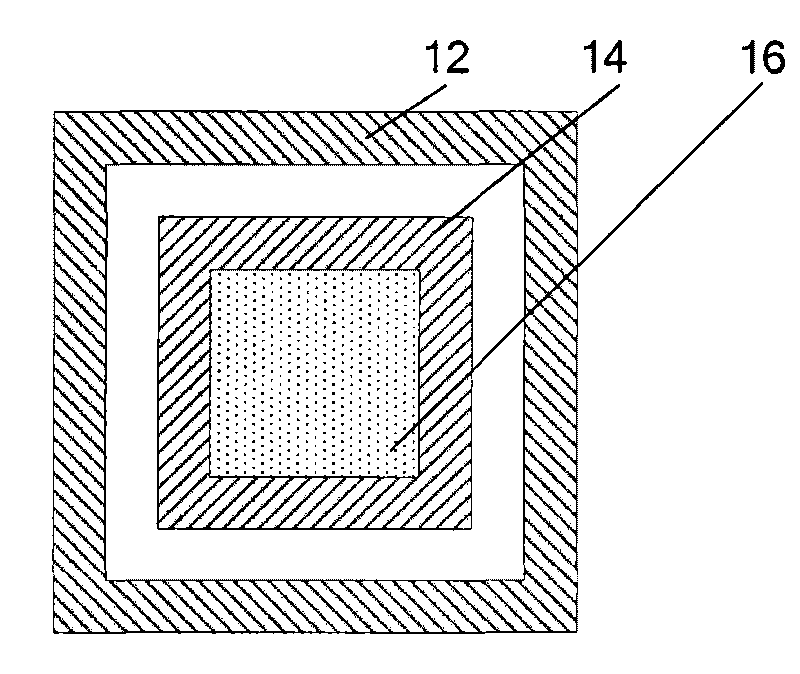
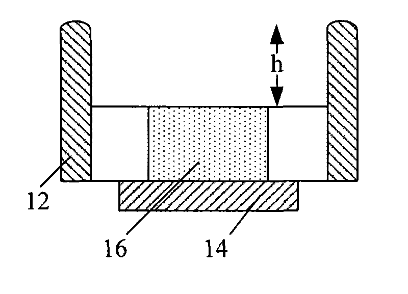
[0017] An embodiment of the present invention provides a chip. The chip includes a plurality of cells of the same shape that are seamlessly connected on a plane. On a plane, the shape of the gate dielectric layer of the cells is larger than the perimeter of the square when the area is the same. Shapes, such as: parallelograms, triangles, trapezoids and other shapes other than squares, these shapes have a perimeter greater than that of a square when they have the same area as a square. The shape of the cell grid dielectric layer 12 is as follows Figure 5 As shown, it is a parallelogram B with an angle between two adjacent sides of 45 degrees or 135 degrees, and the area of ​​the square A parallelogram B is also a 2 , the side length of the square is 4a, and the parallelogram B has a pair of side lengths under the precondition of a, if the area is also a 2 , then the perimeter of the parallelogram B is about 4.828a. Under a certain process, the channel lengths of the square an...


PUM


Abstract

The embodiment of the invention discloses a power device chip and aims to improve the current capability of the power device chip. The chip comprises a plurality of unit cells which are in the same shape and are seamlessly jointed on a plane; a unit cell grid medium layer on the plane is in a shape that the perimeter of the unit cell grid medium layer is larger than the perimeter of a square when the area of the unit cell grid medium layer is same as that of the square, because the ratio of the width to the length of a groove in a unit area is an important factor for deciding the current capability of the chip. Under the condition that the process is fixed, the length of the groove is fixed and the width of the groove is approximately similar to the perimeter of the unit cells, thus the scheme provided by the embodiment of the invention improves the current capability of the power device chip.

Description

technical field [0001] The invention relates to the field of chip manufacturing, in particular to a power device chip. Background technique [0002] At present, the design and manufacture of some chips use cells as the basic structure. For example, the double-diffused metal oxide semiconductor device DMOS is a popular Power MOSFET (Power metallic oxide semiconductor field effect transistor, power transistor) chip manufacturing technology in the semiconductor industry today. Its basic structure is cell. Chips that use cells as the basic structure also include IGBT (Insulated Gate Bipolar Transistor), insulated gate bipolar power transistors, and the like. There are two types of cells: closed cell (closed cell) and striped cell (strip cell). In DMOS design, common closed cells are: such as figure 1 A regular hexagonal cell in the plane as shown, or as figure 2 The square cell shown. The gate dielectric layer 12 is used as a square frame, and Source (source blocking regio...

Claims


Application Information

Patent Timeline
IPC IPC(8): H01L27/02H01L27/088H01L29/78H01L29/423
Inventor 刘鹏飞方绍明陈勇陈洪宁王新强张立荣赵亚民
Owner PEKING UNIV FOUNDER GRP CO LTD
Why Eureka
Try Eureka