Array substrate of thin film transistor and liquid crystal display panel

A technology of liquid crystal display panels and thin film transistors, applied in the direction of electric solid-state devices, semiconductor devices, semiconductor/solid-state device components, etc., can solve the problems of difficult repair lines, narrow spacing, and increased production costs, so as to eliminate line defects and reduce The effect of production cost and production time

Inactive Publication Date: 2010-06-09
华映视讯(吴江)有限公司 +1
View PDF0 Cites 9 Cited by
  • Summary
  • Abstract
  • Description
  • Claims
  • Application Information

AI Technical Summary

Problems solved by technology

However, as the resolution of the panel increases, the distance between two adjacent scan pads 160 or the distance between two adjacent data pads 170 will inevitably become narrower.
Therefore, it is still difficult to repair the damaged circuit by laser cutting, which will reduce the production yield of the thin film transistor array substrate 100 and increase the production cost.

Method used


Image

  • Array substrate of thin film transistor and liquid crystal display panel
  • Array substrate of thin film transistor and liquid crystal display panel
  • Array substrate of thin film transistor and liquid crystal display panel

Examples


Embodiment Construction

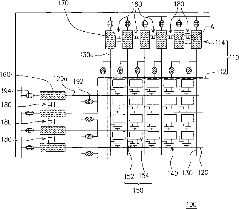
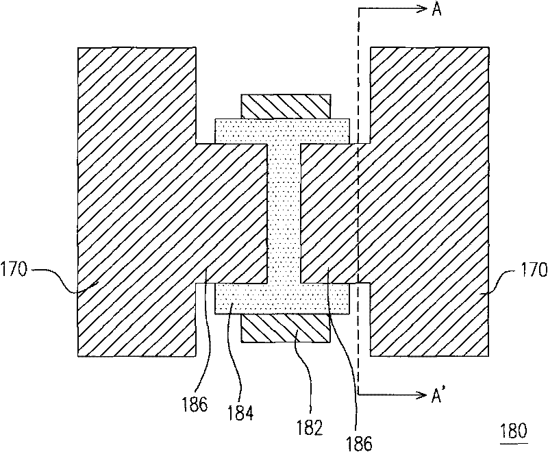
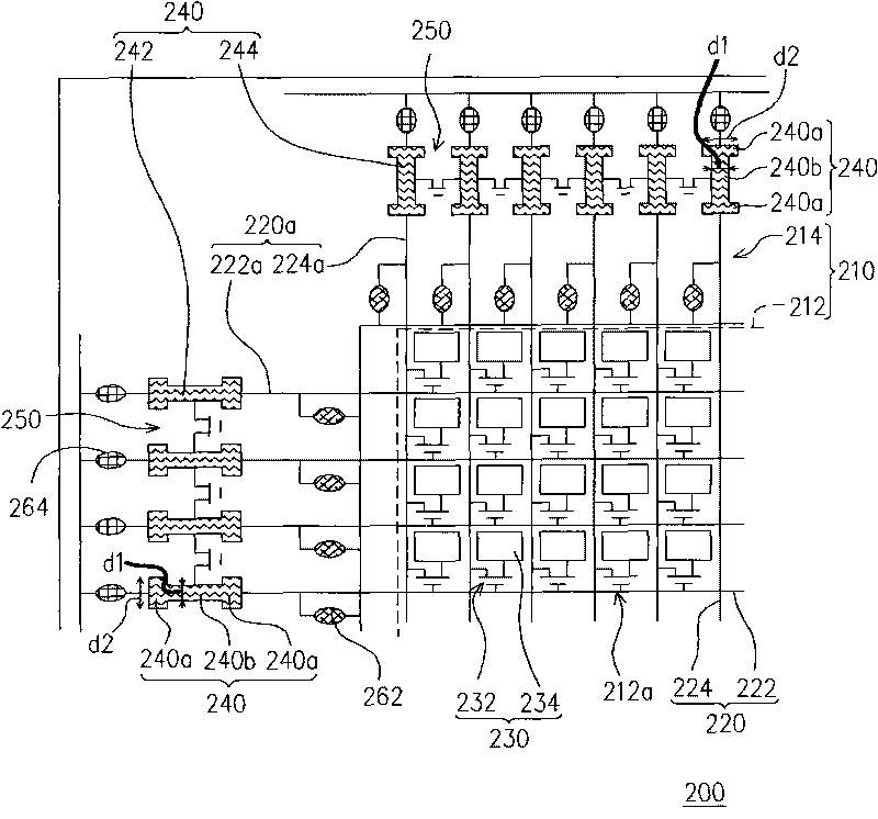
[0056] image 3 A schematic diagram of a thin film transistor array substrate according to a preferred embodiment of the present invention is shown. Please refer to image 3 , the TFT array substrate 200 includes a substrate 210 , a plurality of electrode wires 220 , a plurality of pixel units 230 , a plurality of welding pads 240 and a plurality of switch components 250 .

[0057] The substrate 210 has a display area 212 and a peripheral circuit area 214 . The electrode wiring 220 is disposed on the substrate 210, wherein the electrode wiring 220 divides the display area 212 into a plurality of pixel areas 212a. The electrode wires 220 may include a plurality of scan wires 222 and a plurality of data wires 224 , wherein the scan wires 222 and the data wires 224 are perpendicular to each other.

[0058] The pixel units 230 are respectively disposed in one of the pixel regions 212 a, and are driven by the electrode wiring 220 . Each pixel unit 230 may include: a thin film t...


PUM


Abstract

The invention relates to an array substrate of a thin film transistor, comprising a substrate, a plurality of electrode wirings, a plurality of pixel units, a plurality of pads and a plurality of switch assemblies. The substrate has a display region and a peripheral line region. The electrode wirings are configured on the substrate and divide the display region into a plurality of pixel regions. Each pixel unit is respectively configured in one of the pixel regions and driven by the electrode wirings. The pads are configured in the peripheral line region. Each pad comprises a first main body part and a first extending part. The first extending part is narrower than the first main body part. Each pad is electrically connected with corresponding electrode wiring. The switching assemblies are configured in the peripheral line region, and at least one switch assembly is configured between two adjacent pads. Each switch assembly is electrically connected with the pads on both sides of the switch assembly.

Description

technical field [0001] The present invention relates to an array substrate and a display panel, and in particular to a thin film transistor array substrate (Thin Film Transistor array substrate, TFTarray substrate) which is easy to repair (Electrostatic dischargerepair) the circuit damaged by static electricity and has The liquid crystal display panel (LCD panel) of the thin film transistor array substrate. Background technique [0002] In recent years, due to the maturity of optoelectronic technology and semiconductor manufacturing technology, the flat panel display (Flat Panel Display) has been vigorously developed. Among them, thin film transistor liquid crystal display (ThinFilm Transistor Liquid Crystal Display, TFT-LCD) is based on its low voltage operation, operation speed Due to the advantages of high speed, light weight and small size, it has gradually become the mainstream of display products. [0003] The thin film transistor liquid crystal display mainly include...

Claims


Application Information

Patent Timeline
Patent Type & Authority Applications(China)
IPC IPC(8): H01L27/12H01L23/485G02F1/1362
Inventor 廖淀淦许汉东
Owner 华映视讯(吴江)有限公司
Why Eureka
Try Eureka