Mask plate and manufacture method thereof

A technology of mask plate and light-transmitting area, which is applied in the field of mask plate and its preparation, can solve problems such as uneven exposure of photoresist, uneven photoresist surface, photoresist inclination, over-etching of semiconductor layer, etc., to achieve exposure Uniformity, shorten exposure time, reduce the effect of channel overcut

Active Publication Date: 2010-06-16
K TRONICS (SUZHOU) TECH CO LTD +1
View PDF0 Cites 32 Cited by
  • Summary
  • Abstract
  • Description
  • Claims
  • Application Information

AI Technical Summary

Problems solved by technology

However, this treatment is likely to cause photoresist to remain on the film material corresponding to the region where the photoresist thickness is partially retained. The film material under the photoresist region is not exposed and cannot be etched, and the photoresist region remains. The source-drain metal film or the doped semiconductor layer below is not cut off, so it is easy to form a source-drain short circuit (ie: GT Bridge)
Usually source-drain short circuit is one of the main disadvantages of gray tone mask technology
[0015] In the patterning of the TFT channel, if in order to ensure that the thin film material corresponding to the thick photoresist area can be etched clean, it is easy to make the TFT channel under the thin photoresist part of the photoresist area partially reserved. The exposed semiconductor layer is over-etched, thereby forming a channel over-etch (ie: Channel Open)
[0016] At present, in the process of forming TFT channel patterns based on gray-tone mask technology, source-drain short circuit and channel over-etching defects are two defects that are difficult to avoid at the same time.
The inclination angle a2 of the photoresist 10 remaining on the edge of the TFT channel region formed on the thin film material 20 is small, which affects the final inspection critical dimension (Final Inspection CD, FI-CD) of the TFT channel width and causes defects in the array substrate.
[0018] From the above analysis, it can be seen that in the TFT channel patterning process of the array substrate using the existing gray-tone mask technology and half-tone mask technology, the photoresist on the part of the photoresist reserved area will be exposed unevenly, so that The surface of the photoresist on the partially reserved area of ​​the photoresist is uneven or the dip angle of the photoresist reserved on the edge of the TFT channel is small, which is not conducive to the precise control of the process in the process of forming the TFT channel, and ultimately affects the TFT channel. electrical properties

Method used


Image

  • Mask plate and manufacture method thereof
  • Mask plate and manufacture method thereof
  • Mask plate and manufacture method thereof

Examples


Embodiment Construction

[0046] The technical solutions of the present invention will be described in further detail below with reference to the accompanying drawings and embodiments.

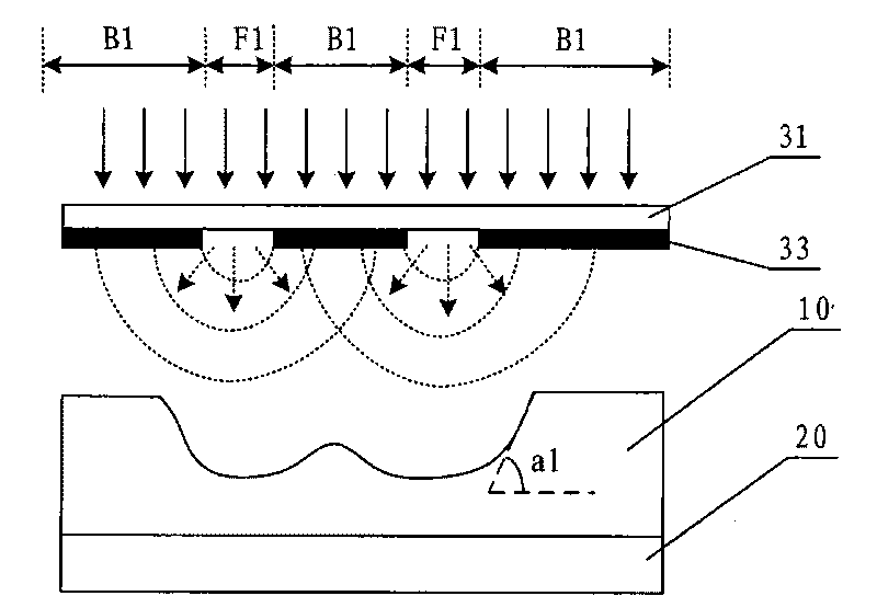
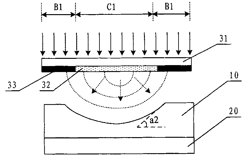
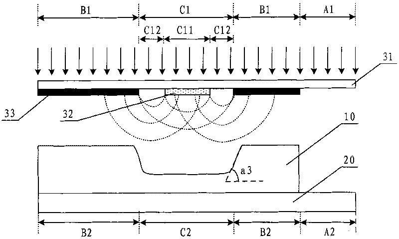
[0047] image 3 It is a schematic diagram of the mask plate of the present invention. The mask plate of the present invention is composed of a transparent substrate 31 , a translucent film 32 and an opaque film 33 , forming a completely transparent area A1 , an opaque area B1 and a partially transparent area C1 . The partially transparent region C1 is formed by alternating translucent parts C11 and transparent parts C12.

[0048] Preferably, the sum of the areas of the translucent parts C11 accounts for 50%-75% of the total area of ​​the partially transparent regions C1. The translucent part C11 may specifically be a translucent film. The transparent part C12 can specifically be the slits formed by the alternate arrangement of translucent films, or the slits formed between the translucent films and the opaque films,...


PUM

PropertyMeasurementUnit
widthaaaaaaaaaa
widthaaaaaaaaaa
widthaaaaaaaaaa

Abstract

The invention relates to a mask plate and a manufacture method thereof. The mask plate comprises a lightproof region, a fully transparent region and a partial transparent region; the partial transparent region is formed in a such way that a semi-transparent part and a transparent part are alternatively arranged. The invention is a new mask plate manufactured by combining a grey mask plate technique and halftone mask plate technique; the mask plate ensures that the exposure of photoresist at the lower part of the partial nonopaque region is uniform when in use, which is beneficial to forming the smooth surface of a partial maintaining region of the photoresist, thereby facilitating the TFT groove etch and improving the yield of array substrates, at the same time, the obliquity of the photoresist at the edge of the partial maintaining region of the photoresist is increased, thereby the technique can be accurately controlled in the process of forming the TFT groove.

Description

technical field [0001] The invention relates to display technology, in particular to a mask plate and a preparation method thereof. Background technique [0002] In order to effectively reduce the cost of Thin Film Transistor Liquid Crystal Display (hereinafter referred to as TFT-LCD) and improve the yield, the manufacturing process of the TFT-LCD array substrate structure is gradually simplified. At present, the 4-time patterning (4Mask) process is gradually being popularized and applied. [0003] The 4th patterning (4Mask) process is the second patterning (for forming semiconductor layer pattern) and the third patterning (for forming source electrode, drain electrode and data line pattern) process in the 5th patterning (5Mask) process Synthesis is achieved through multi-step etching in one patterning process. The 4-time patterning (4Mask) process includes: [0004] Step 11, forming gate electrodes and gate lines on the substrate through a first patterning process. [0...

Claims


Application Information

Patent Timeline
Patent Type & Authority Applications(China)
IPC IPC(8): G03F1/00G03F1/14H01L21/84G03F1/32
Inventor 郝金刚彭志龙朴春培王威
Owner K TRONICS (SUZHOU) TECH CO LTD
Why Eureka
Try Eureka