Etching method

A technology of shielding layer and substrate, applied in the direction of electrical components, semiconductor/solid-state device manufacturing, circuits, etc., can solve problems such as PR pattern error, etching failure, and reduced etching quality, so as to reduce the possibility of etching failure , Improve the etching success rate and improve the etching quality

Inactive Publication Date: 2010-06-16
SEMICON MFG INT (SHANGHAI) CORP
View PDF0 Cites 3 Cited by
  • Summary
  • Abstract
  • Description
  • Claims
  • Application Information

AI Technical Summary

Problems solved by technology

[0008] For the process of 0.18 microns and below, the PR 152 is too thick in the traditional etching scheme, and there will be the following problems: PR collapse (peeling), that is, the problem of PR collapse due to the excessive thickness of PR during etching, such as figure 2 Shown in the circle; and PR residue (scum), that is, because PR is too thick, PR will remain after development, making the formed PR pattern wrong, such as image 3 circled part
The above two problems will cause etching failure
[0009] In order to solve the above problems, the industry proposes to reduce the thickness of PR 152 for etching, for example, reduce the thickness of PR 152 to 5000 angstroms, and adjust the thickness of BARC 151 to 900 angstroms accordingly, but this can solve the problem of PR peeling and PR scum problem, but there are also the following shortcomings: due to the insufficient thickness of PR 152, it will cause excessive etching, expose BARC 151, damage the polysilicon layer that does not need to be etched away, cause the problem of damage to the edge of the fabricated control gate, and reduce the etching quality ,like Figure 4 circled part

Method used


Image

  • Etching method
  • Etching method
  • Etching method

Examples


Embodiment Construction

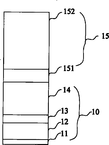
[0027] In view of the problems mentioned in the background technology, the embodiment of the present invention proposes to form a mask layer composed of a shielding layer, a BARC layer and a PR layer on the substrate, and then etch based on the mask layer. Since the mask layer includes the above three layers, it can allow a larger process margin (margin), for example, the thickness of the PR layer can be allowed to have a larger selection range, so even to avoid PR peeling and PR scum, reduce the PR layer Thickness, also can not produce the problem of excessive etching in the prior art, expose BARC, damage the polysilicon layer that does not need to be etched away, cause the edge damage of the manufactured control gate, improve the etching quality.

[0028] Based on the above idea, the embodiment of the present invention proposes the following design method to solve the above problems existing in the existing etching scheme.

[0029] Figure 5 It is a flowchart of an etching ...


PUM


Abstract

The invention provides an etching method for improving etching quality. The method comprises the steps of: providing a substrate; forming a shielding layer, a bottom anti-reflection layer and a photoresist layer on the substrate in sequence to form a mask layer; patterning the mask layer; and etching the substrate on the basis of the patterned mask layer.

Description

technical field [0001] The invention relates to the field of semiconductor manufacturing, in particular to an etching method. Background technique [0002] Etching is a common process in the semiconductor manufacturing process, and its principle is: a mask layer is formed on the wafer; based on the mask layer, the wafer is etched. With the development of semiconductor technology, the critical dimensions of devices are shrinking day by day, and the requirements for etching processes are gradually increasing. refer to figure 1 , figure 1 It is a schematic diagram of part of the structure of the control gate of the flash memory in the existing etching process. The etching process in the production process of the control gate (CG, Control Gate) of the flash memory (Flash) based on the 0.18 micron process includes: [0003] A substrate 10 is provided, which includes a first oxide layer (Oxide) 11, a first polysilicon layer (Poly) 12, a dielectric layer (ONO, SiO-SiN-SiO) 13 an...

Claims


Application Information

Patent Timeline
Patent Type & Authority Applications(China)
IPC IPC(8): H01L21/00H01L21/02H01L21/033H01L21/28
Inventor 李雪
Owner SEMICON MFG INT (SHANGHAI) CORP
Why Eureka
Try Eureka