Method for removing film

A thin film and thin film thickness technology, which is applied in the fields of electrical components, semiconductor/solid-state device manufacturing, circuits, etc., can solve the problems of easy damage to the side wall structure and the underlying structure, and achieve the effect of avoiding damage to the underlying structure and avoiding damage

Inactive Publication Date: 2012-07-18
SEMICON MFG INT (BEIJING) CORP
View PDF2 Cites 0 Cited by
  • Summary
  • Abstract
  • Description
  • Claims
  • Application Information

AI Technical Summary

Problems solved by technology

[0009] The invention provides a thin film removal method to improve the phenomenon that dry etching is easy to damage the underlying structure and wet etching is easy to damage the side wall structure in the existing thin film removal method

Method used


Image

  • Method for removing film
  • Method for removing film
  • Method for removing film

Examples


no. 1 example

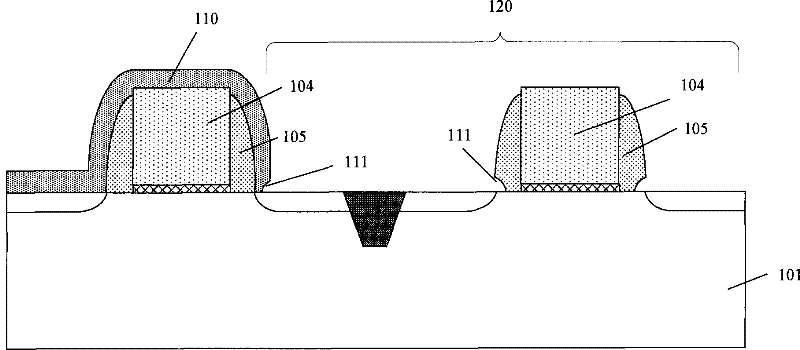
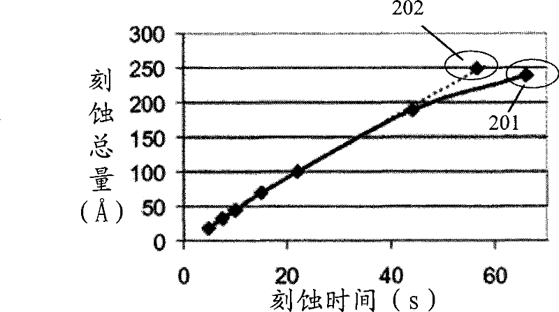
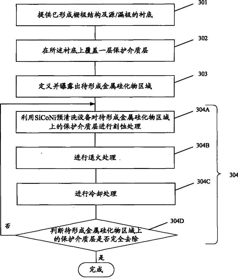
[0125] This embodiment introduces the specific process of removing the protective dielectric layer on the region where the metal silicide is to be formed by using the thin film removing method of the present invention. image 3 It is a flow chart of the thin film removal method for forming localized metal silicide according to the first embodiment of the present invention, Figure 4 to Figure 8 In order to illustrate the device cross-sectional diagram of the thin film removal method for forming localized metal silicides in the first embodiment of the present invention, SiCoNi pre-cleaning equipment is used in this embodiment to realize thin film removal. Combine below Figure 3 to Figure 8 The first embodiment of the present invention will be described in detail.

[0126] Step 301: Provide a substrate on which gate structures and source / drain electrodes have been formed.

[0127] Figure 4 is a schematic cross-sectional view of the substrate provided in the first embodiment...

no. 2 example

[0163] This embodiment introduces the specific process of removing the contact etching stop layer at the bottom of the opening of the contact hole by using the thin film removal method of the present invention. Figure 9 is a flow chart of a thin film removal method for forming a contact hole according to the second embodiment of the present invention, Figure 10 to Figure 15 In order to illustrate the device cross-sectional schematic diagram of the thin film removal method for forming contact holes in the second embodiment of the present invention, the thin film removal in this embodiment is completed by using SiCoNi pre-cleaning equipment, combined below Figure 9 to Figure 15 The second embodiment of the present invention will be described in detail.

[0164] Step 901: Provide a substrate on which a contact etch stop layer has been formed.

[0165] At least one gate structure has been formed on the substrate provided in this embodiment, and a contact etch stop layer has be...


PUM


Abstract

The invention discloses a method for removing a film. The method comprises the following steps of: providing a substrate the surface of which is provided with a film; transmitting the substrate to a treating room; carrying out the plasma activation on reactant gas outside the treating room by using a low-powered radio-frequency power supply; introducing the reactant gas after being subjected to the plasma activation to the treating room; and carrying out etching treatment by using the reactant gas after being subjected the plasma activation to remove the film, and removing resultants producedin the etching treatment process by using the annealing treatment. The invention also discloses specific implementation steps for forming a local metal silicide and forming the opening of a contact hole by using the method correspondingly. By using the method for removing a film, the damage to the understructure by a traditional dry etching method can be avoided, and the damage to the side-wall structure by an isotropic wet corrosion method can be also avoided.

Description

technical field [0001] The invention relates to the technical field of semiconductor manufacturing, in particular to a thin film removal method. Background technique [0002] The process of manufacturing semiconductor integrated circuit chips uses batch processing technology to form a large number of various types of complex devices on the same silicon substrate and connect them to each other to have complete electronic functions. With the rapid development of ultra-large-scale integrated circuits, the integration of chips is getting higher and higher, and the size of components is getting smaller and smaller. The various effects caused by the high density and small size of devices have an increasing impact on the results of semiconductor process manufacturing. protrude. [0003] For example, as the feature size of VLSI devices is continuously reduced proportionally and the integration level is continuously improved, the process requirements for removing various thin films ...

Claims


Application Information

Patent Timeline
Patent Type & Authority Patents(China)
IPC IPC(8): H01L21/00H01L21/02H01L21/311H01L21/768
Inventor 何伟业苏娜杨瑞鹏
Owner SEMICON MFG INT (BEIJING) CORP
Why Eureka
Try Eureka