Supercharge Your Innovation With Domain-Expert AI Agents!

Processing procedure of semiconductor manufactured aluminium metal wire

An aluminum metal and semiconductor technology, which is applied in the field of semiconductor manufacturing aluminum metal wire process, can solve the problems of expanding and expanding the operating voltage and voltage difference, short circuit, etc., to avoid tip discharge and reduce charge accumulation.

Active Publication Date: 2010-06-16
SHANGHAI HUAHONG GRACE SEMICON MFG CORP
View PDF0 Cites 0 Cited by
  • Summary
  • Abstract
  • Description
  • Claims
  • Application Information

AI Technical Summary

Problems solved by technology

[0007] like figure 2 As shown, in the specific design rules, due to the aluminum metal in the large isolated area used in the design layout, such as Vpwr (power supply terminal) and Vpos (positive terminal), and Vpwr is floating (suspension), there is no Connected to the Sub (substrate), resulting in the accumulation of charges during the IMD deposition process that cannot be released on the bulk aluminum metal connected to Vpwr, thus expanding the voltage difference caused by the operating voltage
From the cross-section of the metal, because these metals are surrounded by open areas, the bottom of the cross-section is conical, and the tip discharge caused by the antenna effect will occur from the bottom (the area shown by the dotted line in the figure), and the charge accumulation during the IMD deposition process is expanded. Eliminates the tip discharge effect caused by the smaller spacing between metal lines, which can easily lead to a short circuit between Vpos and Vpwr, reducing product yield

Method used


Image

  • Processing procedure of semiconductor manufactured aluminium metal wire
  • Processing procedure of semiconductor manufactured aluminium metal wire
  • Processing procedure of semiconductor manufactured aluminium metal wire

Examples


Embodiment Construction

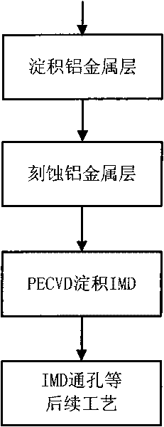
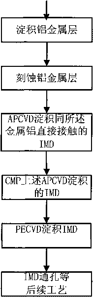
[0022] An embodiment of the semiconductor manufacturing aluminum metal wire process of the present invention is as follows image 3 shown, including the following steps:

[0023] 1. Deposit aluminum metal film;

[0024] 2. Etching the aluminum metal film;

[0025] 3. APCVD (atmospheric pressure chemical vapor deposition) deposits IMD (such as TEOS, orthoethyl silicate) in direct contact with the metal aluminum;

[0026] 4. CMP (Chemical Mechanical Polishing) IMD deposited by APCVD above;

[0027] 5. PECVD deposition IMD;

[0028] 6. Subsequent processes such as IMD through holes.

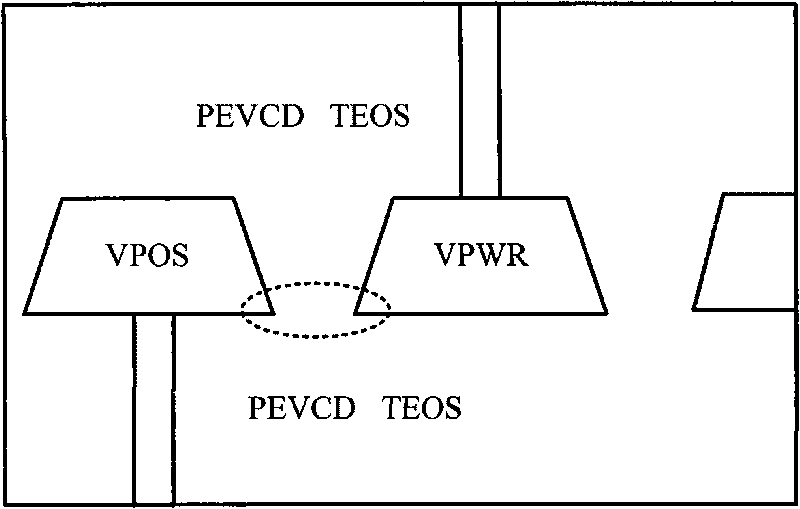
[0029] The semiconductor sectional view of the aluminum metal wire manufacturing process adopting the semiconductor of the present invention is as Figure 4 As shown, APCVD (atmospheric pressure chemical vapor deposition) was used to deposit the IMD in direct contact with the aluminum metal.

[0030] In the semiconductor manufacturing aluminum metal wire process of the present invention, after...


PUM


Abstract

The invention discloses a processing procedure of a semiconductor manufactured aluminium metal wire, comprising the following steps of: depositing an aluminium metal thin film; etching the aluminium metal thin film; depositing in-mold decoration (IMD) directly touching metal aluminium by atmospheric pressure chemical vapor deposition (APCVD); and depositing the IMD by plasma enhanced chemical vapor deposition (PECVD). The processing procedure of the semiconductor manufacturing aluminium metal wire can reduce the plasma damage in the processing procedure of the aluminium metal wire, and increases the product yield.

Description

technical field [0001] The invention relates to a semiconductor manufacturing process, in particular to a semiconductor manufacturing aluminum metal wire manufacturing process. Background technique [0002] In the metallization process of semiconductor manufacturing, aluminum metal is used as the back-end connection. For example, in the 0.13um process, due to the shrinkage of the design rules, the space (spacing) between the aluminum metal lines is small, and the higher operating voltage will increase. The breakdown probability between aluminum and other metal wires, the current semiconductor manufacturing aluminum metal wire process, such as figure 1 shown, including the following steps: [0003] 1. Deposit aluminum metal film; [0004] 2. Etching the aluminum metal film; [0005] 3. PECVD (Plasma Enhanced Chemical Vapor Deposition) deposits IMD (Inter-Metal Dielectric, inter-metal dielectric layer); [0006] 4. Subsequent processes such as IMD through holes. [0007] ...

Claims


Application Information

Patent Timeline
IPC IPC(8): H01L21/768
Inventor 谭颖陈广龙
Owner SHANGHAI HUAHONG GRACE SEMICON MFG CORP
Features
  • R&D
  • Intellectual Property
  • Life Sciences
  • Materials
  • Tech Scout
  • Unparalleled Data Quality
  • Higher Quality Content
  • 60% Fewer Hallucinations
Learn More