Polycrystalline silicon electric resistance and manufacturing method thereof

A polysilicon resistor and manufacturing method technology, applied in circuits, electrical components, electrical solid devices, etc., can solve the problems of large occupied area and disadvantageous chip cost, and achieve the effect of saving cost and reducing chip occupied area.

Active Publication Date: 2010-06-16
SHANGHAI HUAHONG GRACE SEMICON MFG CORP
View PDF0 Cites 10 Cited by
  • Summary
  • Abstract
  • Description
  • Claims
  • Application Information

AI Technical Summary

Problems solved by technology

That is to say, polysilicon should meet the design rules of Layout. For polysilicon with a width of L, there must be a certain distance S between every two polysilicons. Therefore, the structure occupies a large area, which is not conducive to controlling the cost of chip design.

Method used


Image

  • Polycrystalline silicon electric resistance and manufacturing method thereof
  • Polycrystalline silicon electric resistance and manufacturing method thereof
  • Polycrystalline silicon electric resistance and manufacturing method thereof

Examples


Embodiment Construction

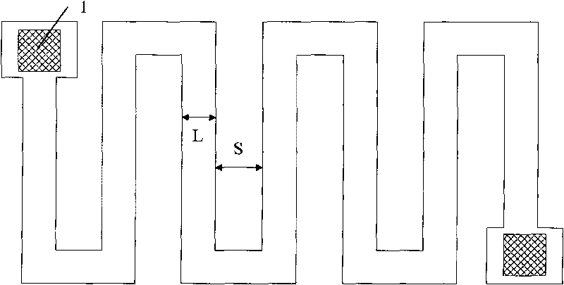
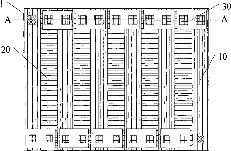
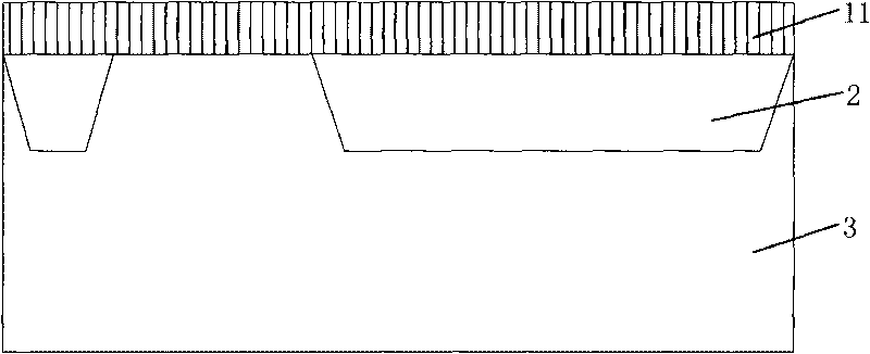
[0028] Such as figure 2 , Figure 9 As shown, the polysilicon resistance of the present invention includes double-layer polysilicon, namely the first layer of polysilicon 10 and the second layer of polysilicon 20, the two layers of polysilicon 10,20 are distributed up and down, and an insulating layer 40 is arranged between the two layers of polysilicon 10,20; The layers of polysilicon 10 and 20 are connected to the first layer metal line 30 through the contact hole 1 . Figure 9 for figure 2 Sectional view of A-A in the middle.

[0029] The insulating layer 40 may be silicon oxide, silicon nitride or a combination thereof. The function of the insulating layer 40 is to isolate the upper and lower layers of polysilicon 10 and 20 .

[0030] The manufacturing process method of polysilicon resistance of the present invention, forms polysilicon resistance by following steps:

[0031] 1. If image 3 As shown, on the P-type substrate 3, the non-doped first layer of polysilico...


PUM


Abstract

The invention discloses a polycrystalline silicon electric resistance, comprising two layers of polycrystalline silicon which are arranged from top to bottom, an insulation layer is arranged between the two layers of polycrystalline silicon; the two layers of polycrystalline silicon are connected with a first layer of metal wire through contact holes. The insulation layer is silicon oxide or silicon nitride or the combination of silicon oxide and silicon nitride. In the invention, the two layers of polycrystalline silicon are adopted to change a plane polycrystalline silicon electric resistance into a two-layered up-and-down three-dimensional structure, a layer of insulation layer is used for segregating the two layers of polycrystalline silicon; in addition, the two layers of polycrystalline silicon are connected with the first layer of metal wire through the contact holes, so that 50% of chip-occupied area can be saved and the cost can be greatly reduced; moreover the structure enjoys more advantages when being applied to manufacture large polycrystalline silicon electric resistance. The invention also discloses a manufacturing method of the polycrystalline silicon electric resistance.

Description

technical field [0001] The invention relates to a semiconductor structure, in particular to a polysilicon resistor, and also relates to a manufacturing method of the polysilicon resistor. Background technique [0002] According to R=(p / t)(L / W)=R □ (L / W), if you want to make a large polysilicon resistor, you must design the polysilicon resistor as figure 1 In the long strip structure shown, there is a contact hole 1 on the polysilicon resistor. That is to say, the polysilicon should meet the design rules of layout. For polysilicon with a width of L, there must be a certain distance S between each two polysilicons. Therefore, the structure occupies a large area, which is not conducive to controlling the cost of chip design. Contents of the invention [0003] The technical problem to be solved by the present invention is to provide a polysilicon resistor, which can save the occupied area of ​​the chip and control the cost of chip design. [0004] For solving the problems o...

Claims


Application Information

Patent Timeline
Patent Type & Authority Applications(China)
IPC IPC(8): H01L29/86H01L27/02H01L21/02H01L21/8238H01L21/768
Inventor 陈华伦熊涛陈瑜陈雄斌罗啸
Owner SHANGHAI HUAHONG GRACE SEMICON MFG CORP
Why Eureka
Try Eureka