Method for shrinking line-shaped pattern character size

A technology of pattern features and feature size, applied in electrical components, semiconductor/solid-state device manufacturing, circuits, etc., can solve problems such as cost increase, etching deviation difference, inability to ensure device feature size uniformity, etc., to ensure uniformity, reduce effect of difference

Inactive Publication Date: 2010-06-23
SEMICON MFG INT (SHANGHAI) CORP
View PDF0 Cites 15 Cited by
  • Summary
  • Abstract
  • Description
  • Claims
  • Application Information

AI Technical Summary

Problems solved by technology

Therefore, the existing technology uses a deep ultraviolet light scanner with a wavelength of 193nm to define the graphics with the above-mentioned characteristic dimensions, but this will inevitably increase the cost and reduce the competitiveness of the product. powerful and inexpensive method to achieve smaller line-type feature sizes
[0005] In order to solve the problem of high cost caused by using a light source with a shorter wavelength to shrink the feature size of the line pattern, a method for shrinking the feature size of the line pattern is provided. The method is used in a dry etching process, and the above-mentioned 0.13um DRAM Take the product as an example. First, in order to obtain a bit line with a feature size of 0.07um, a deep ultraviolet scanner with a photoresist with a feature size of 0.105um is used to define the pattern. instrument; subsequently, dry etching the photoresist pattern as a mask, the etching gas contains oxygen, carbon monoxide and nitrogen, etc., in this step, the feature size of the photoresist can be reduced by about 30nm due to isotropic etching; finally Etching the bit line metal of DRAM, in this step, the feature size of the photoresist will be reduced by about 5nm again, and finally a bit line with a feature size of 0.07um will be obtained
However, due to the serious micro-loading effect in the above-mentioned process of using the photoresist pattern as a mask for dry etching, the etching deviation at different densities in the photoresist pattern has a large difference, and because it is difficult to quantify Correlation between pattern density and etch variation, so device feature size uniformity cannot be guaranteed

Method used


Image

  • Method for shrinking line-shaped pattern character size
  • Method for shrinking line-shaped pattern character size
  • Method for shrinking line-shaped pattern character size

Examples


Embodiment Construction

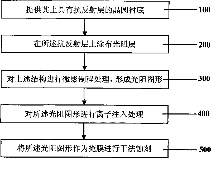
[0029] In order to better understand the technical content of the present invention, specific embodiments are described in conjunction with the accompanying drawings as follows.

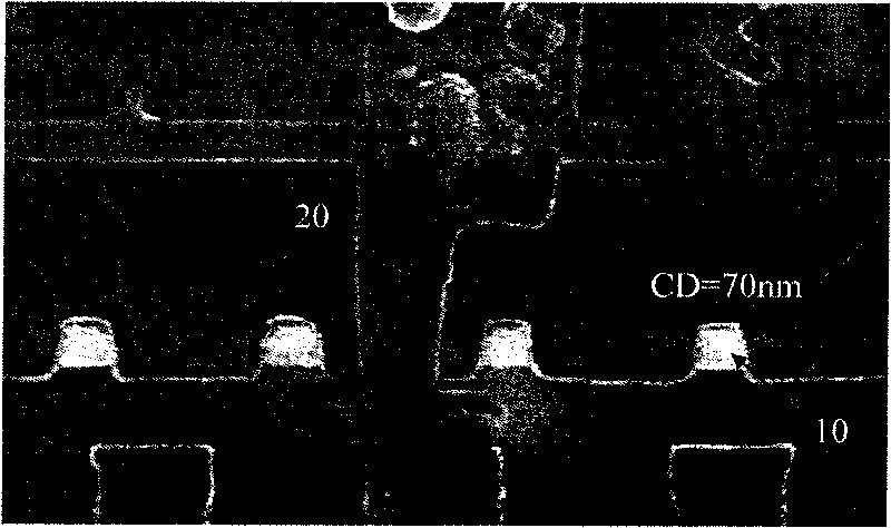
[0030] The present invention provides a method for shrinking the feature size of a linear pattern, which can effectively shrink the feature size of the photoresist, ensure the uniformity of the feature size of the device on the entire wafer, and make the roughness of the linear edge of the photoresist smoother .

[0031] The method for shrinking the feature size of the linear pattern includes: performing ion implantation on the photoresist pattern as a mask to shrink the feature size of the photoresist pattern.

[0032] Through ion implantation of the photoresist pattern as a mask, not only the feature size of the photoresist pattern can be reduced, but also the etching resistance of the photoresist pattern in the subsequent etching process can be increased. Therefore, the photoresist In the process where ...


PUM


Abstract

The present invention provides a method for shrinking line-shaped pattern character sizes, which comprises the following step: irons are injected to a photoresistive pattern as a mask to enable the character size of the photoresistive pattern to shrink. The method for shrinking line-shaped pattern character sizes can effectively shrink the character size of the photoresistive pattern to enable the roughness concentration of a photoresistive linear boundary to become smoother and ensure the uniformity of the character size of the whole wafer. After the processing of iron injection, the anti-etching ability of photoresistance in a subsequent etching process is largely strengthened, and the difference (that is micro load effect) of an intensive pattern and a thin pattern on the reduction of the character size is effectively reduced.

Description

Technical field [0001] The present invention relates to the field of semiconductor integrated circuit manufacturing, and in particular to a method for shrinking the feature size of a line pattern. Background technique [0002] With the rapid development of semiconductor technology, the size of integrated circuit device designs continues to develop in the direction of miniaturization. Based on market competition and industrial demand, continuously improving the performance / price ratio of products is the driving force for the development of microelectronics technology. The characteristic dimension, namely the critical dimension (CD), refers to the minimum wire width that can be achieved by the integrated circuit chip process, and is the smallest dimension that can be processed in a process line, and it is the main indicator of the advanced level of integrated circuit chip technology. The smaller the line width, the higher the degree of integration, and more chips can be integrated...

Claims


Application Information

Patent Timeline
Patent Type & Authority Applications(China)
IPC IPC(8): H01L21/00H01L21/3115H01L21/027
Inventor 罗飞邹立
Owner SEMICON MFG INT (SHANGHAI) CORP
Why Eureka
Try Eureka