Electronic element wafer module and, optical element wafer module and method for manufacturing same

A technology of electronic components and optical components, applied in the direction of electrical components, semiconductor/solid-state device manufacturing, electronic equipment, etc., can solve problems such as poor manufacturing efficiency, achieve low cost, high manufacturing efficiency, and realize the effect of cumulative cost

Inactive Publication Date: 2010-06-23
SHARP KK
View PDF1 Cites 11 Cited by
  • Summary
  • Abstract
  • Description
  • Claims
  • Application Information

AI Technical Summary

Problems solved by technology

This results in very poor manufacturing efficiencies

Method used


Image

  • Electronic element wafer module and, optical element wafer module and method for manufacturing same
  • Electronic element wafer module and, optical element wafer module and method for manufacturing same
  • Electronic element wafer module and, optical element wafer module and method for manufacturing same

Examples


Embodiment 1

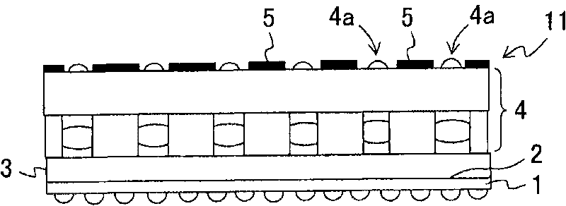
[0052] (Example 1) figure 1 is a longitudinal sectional view showing an exemplary basic component structure of a sensor wafer module according to Embodiment 1 of the present invention.

[0053] exist figure 1Among them, the sensor wafer module 11 according to Embodiment 1 includes: a sensor wafer 1 in which an image capture element is provided as an electronic element on the wafer surface, and the image capture element is composed of a plurality of photoelectric conversion parts respectively corresponding to a plurality of pixels The light receiving part of (photodiode) is constituted, and a through hole is provided between the front surface and the rear surface for electrical connection; the resin adhesive layer 2 formed around the image capturing element of the sensor wafer 1; A cover glass glass plate 3 to cover the image capture element and resin adhesive layer 2; disposed on the glass plate 3 and including one or more laminates therein as used to focus incident light o...

Embodiment 2

[0080] (Embodiment 2) Embodiment 1 describes a case in which a lens wafer module 4 is laminated on a module TSV, and then an optical aperture is formed by a light shielding film 5 at each light opening 4 a of the lens wafer module 4 . Whereas Embodiment 2 describes the case where instead of laminating the lens wafer module 4 on the module TSV, an optical aperture is formed by the light shielding film 5 at each light opening 4a of the lens wafer module 4, and then the lens wafer module 4A is stacked on the module TSV.

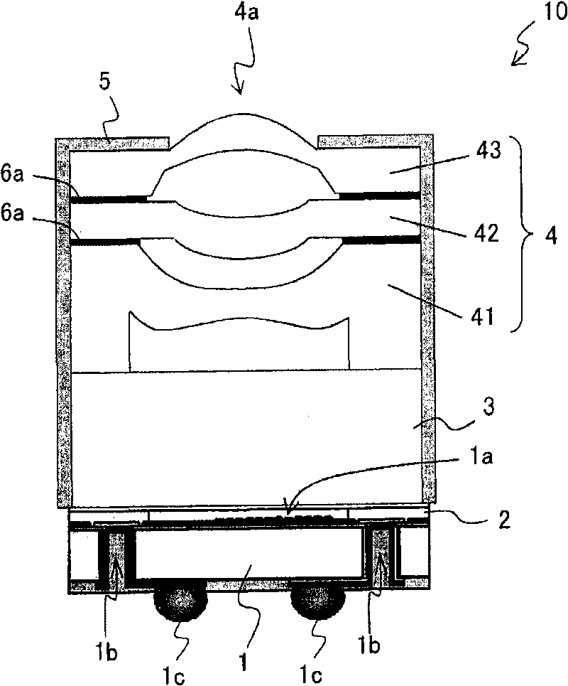
[0081] Figure 7 is a longitudinal sectional view showing an exemplary basic component structure of a lens wafer module 4A according to Embodiment 2 of the present invention.

[0082] exist Figure 7 Among them, the lens wafer module 4A according to Embodiment 2 includes a lens wafer module 4 (in which one or more lens plates are laminated as an optical element for focusing incident light onto an image capturing element), and a The light-shielding film 5 in t...

Embodiment 3

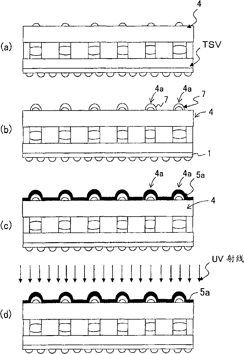
[0103] (Embodiment 3) Embodiment 2 describes the case where instead of laminating the lens wafer module 4 on the module TSV, the low-viscosity protective resin film 7 and the The light-shielding film 5 forms an optical aperture in the light-shielding film 5, and then the lens wafer module 4A is laminated on the module TSV. Whereas in Embodiment 3, a case is described in which the soluble protective resin film 7A on the light opening 4a of the lens wafer module 4 is dissolved to be removed and passed through the lens wafer module 4 before laminating the lens wafer module 4 on the module TSV. The light-shielding film 5 forms an optical aperture, and then, the lens wafer module 4 is laminated on the module TSV.

[0104] will refer to Figure 12 (a) to 12(d) and Figure 13 (a) to 13(d) describe in detail another example of the method of manufacturing the lens wafer module 4A having the above structure.

[0105] First, if Figure 12 As shown in the lamination step of (a), a plu...


PUM


Abstract

The present invention relates to an electronic element wafer module and a method for manufacturing the same; an electronic element module; an optical element wafer module and a method for manufacturing the same; and an electronic information device. A method for manufacturing an electronic element wafer module is provided, the method comprising: a protective resin film forming step of forming a protective resin film on only light openings of the plurality of wafer-shaped optical elements; a light shielding film forming step of filming a light shielding film on an area except for the light openings or an entire area including the light openings; and an optical aperture forming step of removing the protective resin film, or removing the protective resin film and a light shielding film material on the protective resin film, to form an optical aperture structure by the light shielding film at the light openings.

Description

[0001] This non-provisional application claims priority under 35 U.S.C. §119(a) to Patent Application No. 2008-306876 filed in Japan on December 1, 2008, the entire contents of which are hereby incorporated by reference. technical field [0002] The present invention relates to: an electronic element wafer module with an optical aperture structure and a method for manufacturing the electronic element wafer module; an optical element wafer module for the electronic element wafer module and a method for manufacturing the optical element wafer module; Electronic component modules individualized by simultaneously cutting said electronic component wafer modules; and electronic information devices such as digital cameras (such as digital video cameras or digital still cameras), image input cameras (such as surveillance cameras), scanners, facsimile TV sets, TV telephone equipment, and camera-equipped cellular phone sets, including electronic component modules used as image input mean...

Claims


Application Information

Patent Timeline
Patent Type & Authority Applications(China)
IPC IPC(8): H01L21/50H01L21/56H01L27/146
CPCH01L27/14618H01L27/14683H04N5/2257B32B2457/14H01L2924/0002H04N23/57H01L2924/00
Inventor 末武爱士
Owner SHARP KK
Why Eureka
Try Eureka