Compact semiconductor package with integrated bypass capacitor and method

A technology of semiconductors and capacitors, which is applied in the direction of semiconductor devices, semiconductor/solid-state device manufacturing, semiconductor/solid-state device components, etc. It can solve the problems of no large-scale top exposure and limited structural details of the input capacitor Cin

Active Publication Date: 2010-06-23
重庆万国半导体科技有限公司
View PDF11 Cites 14 Cited by
  • Summary
  • Abstract
  • Description
  • Claims
  • Application Information

AI Technical Summary

Problems solved by technology

From the photos provided in the IEEE paper, although there are limited structural details about how the input capacitor Cin is mounted on the top of the system-in-package, there is no evidence that the system-in-package is used to increase the heat dissipation on the top of the input capacitor. The top exposure of the miniature contact holes outside the
Another conclusion is that the system-in-package described in the IEEE paper does not have extensive top exposure above the high-side and low-side MOSFET chips, except for the end of the input capacitor Cin.

Method used


Image

  • Compact semiconductor package with integrated bypass capacitor and method
  • Compact semiconductor package with integrated bypass capacitor and method
  • Compact semiconductor package with integrated bypass capacitor and method

Examples


Embodiment Construction

[0058] The foregoing and following descriptions and drawings contained herein focus only on one or more presently preferred embodiments of the invention and illustrate some typical alternatives and / or alternative embodiments. Accordingly, the description and drawings are intended to be illustrative only and are not intended to limit the scope of the present invention. Various changes, modifications, and substitutions can be easily identified by those skilled in the art. These changes, modifications and substitutions should be considered to belong to the protection scope of the present invention.

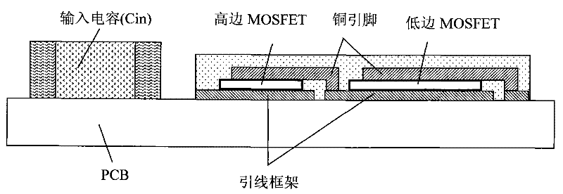
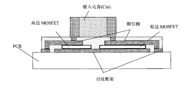
[0059] figure 2 A first part of semiconductor package 500 including semiconductor chip one 520a and semiconductor chip two 520b is shown in the present invention. The first part of the semiconductor package 500 includes:

[0060] A circuit substrate, i.e. lead frame 502 in this figure, contains several terminal leads 506a and 506b for external electrical connection;

[0061] The...


PUM


Abstract

A top-side cooled compact semiconductor package with integrated bypass capacitor is disclosed. The top-side cooled compact semiconductor package includes a circuit substrate with terminal leads, numerous semiconductor dies bonded atop the circuit substrate, numerous elevation-adaptive interconnection plates for bonding and interconnecting top contact areas of the semiconductor dies with the circuit substrate, a first member of the elevation-adaptive interconnection plates has a first flat-top area and a second member of the elevation-adaptive interconnection plates has a second flat-top area in level with the first flat-top area, a bypass capacitor, having two capacitor terminals located at its ends, stacked atop the two interconnection plate members while being bonded thereto via the first flat-top area and the second flat-top area for a reduced interconnection parasitic impedance.

Description

technical field [0001] The invention relates to the field of electronic system packaging. More precisely, the invention applies to physical level packaging of semiconductor wafers. Background technique [0002] Due to its high integration density, relatively low static leakage current and increasing power capacity, power MOSFETs are still widely used in power electronics such as switching power supplies and frequency converters. Moreover, power mosfets also have many very important characteristics, such as: increasing integration, decreasing package size and the consequent increasing requirements for heat dissipation in the consumer market. [0003] Listed below are some related prior art references in US application 12 / 326,065: [0004] "DirectFET" technology (US Patent 6,624,522, US Patent 7,285,866 and US Patent Application Publication 2007 / 0284722); [0005] US Patent 6,777,800 entitled "Semiconductor Chip Package Including Drain Clip"; [0006] U.S. application 11 / 7...

Claims


Application Information

Patent Timeline
Patent Type & Authority Applications(China)
IPC IPC(8): H01L25/00H01L23/48H01L23/52H01L23/31H01L21/50H01L21/60H01L21/56
CPCH01L2224/32245H01L2924/10329H01L24/34H01L2924/01005H01L2224/73265H01L2224/48465H01L2924/13091H01L2924/30107H01L2924/19041H01L2924/13055H01L2924/3011H01L2924/1305H01L2924/181H01L2224/40245H01L24/40H01L2924/14H01L2224/37011H01L2224/73221H01L2224/40H01L2924/00014H01L2224/37H01L2224/83801H01L2224/0603H01L24/84H01L2224/84801H01L2224/8485H01L2224/4103H01L2224/48247H01L2924/00H01L2924/00012H01L2224/37099H01L2224/37599
Inventor 弗兰茨娃·赫尔伯特刘凯
Owner 重庆万国半导体科技有限公司
Why Eureka
Try Eureka