Heat treatment device and method

A heat treatment method and heat treatment device technology, applied in electrical components, semiconductor/solid-state device manufacturing, circuits, etc., can solve the problem that the heat treatment process cannot reduce the heat treatment duration, etc., and achieve the effect of precise control of thermal budget and effective control

Inactive Publication Date: 2010-06-30
SEMICON MFG INT (SHANGHAI) CORP +1
View PDF1 Cites 3 Cited by
  • Summary
  • Abstract
  • Description
  • Claims
  • Application Information

AI Technical Summary

Problems solved by technology

[0010] The invention provides a heat treatment device and method to solve the problem that the existing heat treatment process cannot reduce the duration of heat treatment

Method used


Image

  • Heat treatment device and method
  • Heat treatment device and method
  • Heat treatment device and method

Examples


Embodiment Construction

[0039] The specific embodiments of the present invention will be described in detail below in conjunction with the accompanying drawings.

[0040] In the following description, numerous specific details are set forth in order to provide a thorough understanding of the present invention. However, the present invention can be implemented in many other ways different from those described here, and those skilled in the art can make similar extensions without violating the connotation of the present invention, so the present invention is not limited by the specific implementations disclosed below.

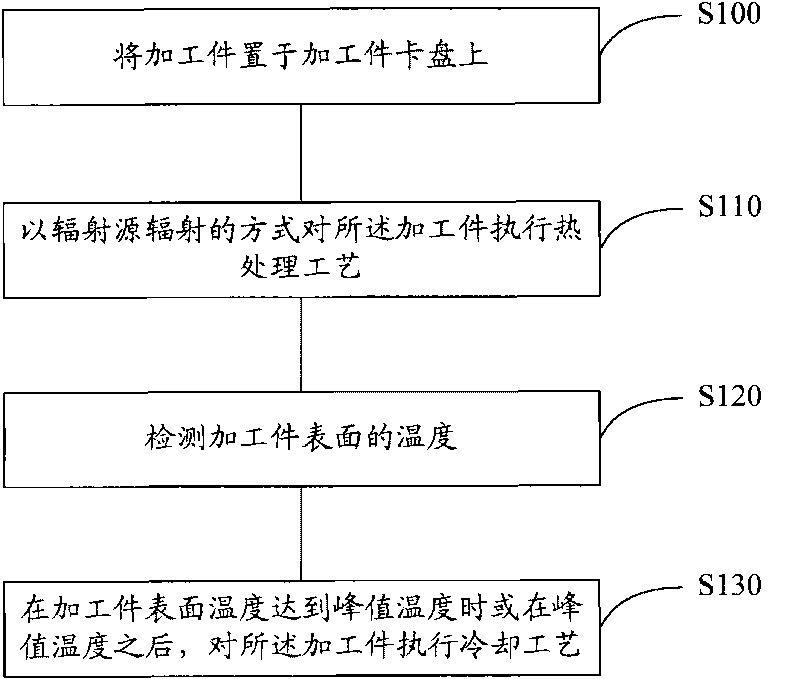
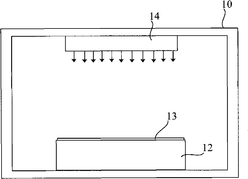
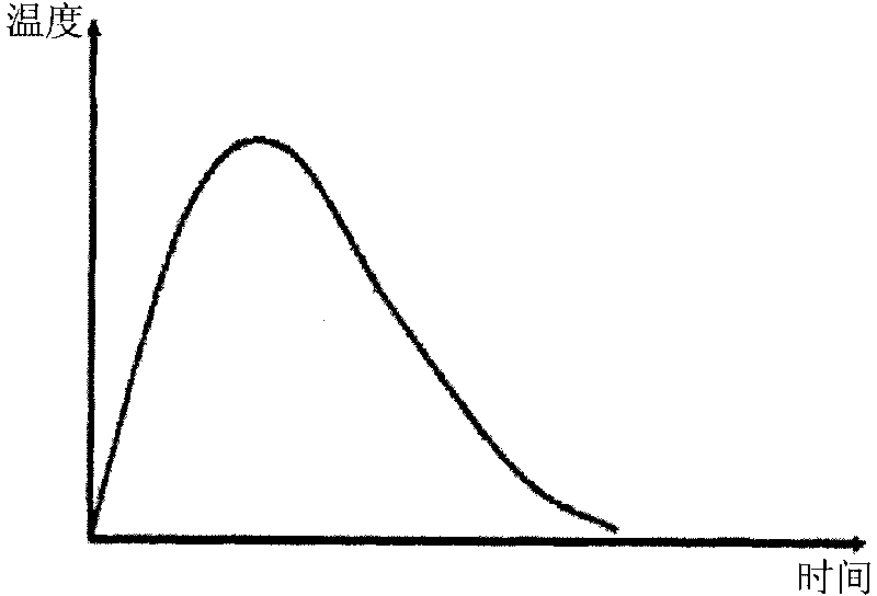
[0041] In the manufacturing process of semiconductor integrated circuits, rapid heat treatment process is commonly used for heat treatment. For example, in the shallow junction manufacturing process, after ion implantation, rapid heat treatment is required to activate the implanted ions and repair the implantation damage; in the metal silicide manufacturing process, a rapid heat treatme...


PUM


Abstract

The invention discloses a heat treatment method. In the method, a workpiece is arranged on a workpiece chuck; heat treatment is carried out on the workpiece in a radiating manner of a radiation source; finally, the workpiece is cooled when the surface temperature of the workpiece reaches or lags behind the peak temperature. The invention further provides a heat treatment device. The invention can shorten the heat treatment time of the workpiece in order to change the heat treatment effect of the workpiece, is beneficial for accurately controlling the heat budget, and can adjust the heat treatment time according to need.

Description

technical field [0001] The invention relates to the technical field of semiconductor manufacturing, in particular to a heat treatment device and method. Background technique [0002] The thermal annealing process is widely used in the manufacturing process of semiconductor integrated circuits. For example, a thermal annealing process is used to activate the implanted ions after ion implantation, and a thermal annealing process is used to change stress in a strained silicon manufacturing process. [0003] With the improvement of integration and the reduction of device size, the requirements for thermal annealing process are getting higher and higher. For example, the annealing time needs to be strictly controlled, and the thermal budget is reduced due to the reduction of devices. Based on this, the industry introduces a flash annealing (Flash Anneal) process. The flash annealing process refers to the process of using a radiation source to irradiate a workpiece (such as a se...

Claims


Application Information

Patent Timeline
IPC IPC(8): H01L21/00H01L21/324
Inventor 吴汉明王国华
Owner SEMICON MFG INT (SHANGHAI) CORP
Why Eureka
Try Eureka