Method for preparing transmission electron microscope detecting sample wafer

An electron microscope and sample technology, which is applied in the fields of material analysis and semiconductor manufacturing, can solve the problems of the polymer mask 10 destroying the extra carbon-containing layer, etc., and achieve the effect of increasing the protection ability, reducing the error and improving the quality.

Inactive Publication Date: 2010-07-14
SEMICON MFG INT (SHANGHAI) CORP
View PDF0 Cites 15 Cited by
  • Summary
  • Abstract
  • Description
  • Claims
  • Application Information

AI Technical Summary

Problems solved by technology

[0017] The present invention first deposits the barrier layer on the initial TEM detection sample; then deposits the electron beam auxiliary layer and the ion beam auxiliary layer in sequence, which increases the protection ability of the initial TEM detection sample, an

Method used


Image

  • Method for preparing transmission electron microscope detecting sample wafer
  • Method for preparing transmission electron microscope detecting sample wafer
  • Method for preparing transmission electron microscope detecting sample wafer

Examples


preparation example Construction

[0025] Figure 4 It is a flowchart of a method for preparing a TEM detection sample in an embodiment of the present invention. In combination with this figure, the method includes:

[0026] Step 1, provide initial TEM detection samples;

[0027] The initial TEM inspection sample is obtained after dicing the wafer.

[0028] Step 2, depositing a barrier layer on the initial TEM detection sample;

[0029] The barrier layer can be made of various materials, such as platinum (Pt), platinum-palladium (Pt-Pd) alloy, palladium (Pd), gold (Au) or chromium (Cr), etc.; the barrier layer is usually deposited by physical vapor deposition Process (PVD) deposition, of course, if the deposition of the barrier layer can be achieved and the conventional requirements for sample preparation are met, other processes can also be used;

[0030] In order to realize effective protection for the initial TEM detection sample, it should be ensured that the barrier layer completely covers the surface o...

Embodiment

[0041] Taking the production of the TEM detection sample of the background technology as an example, the preparation process of this embodiment includes:

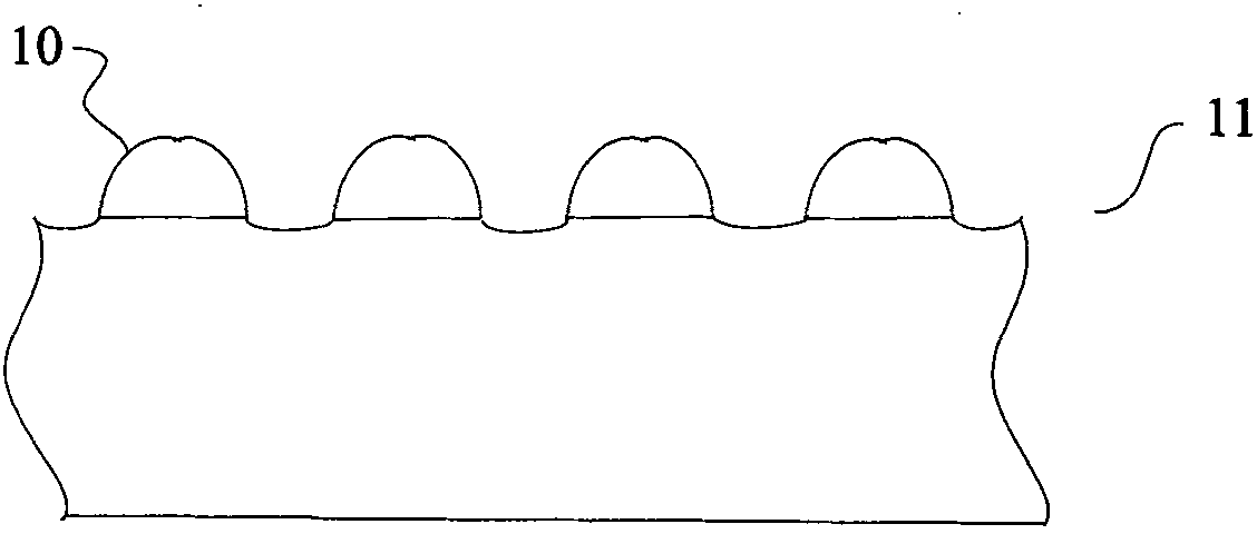
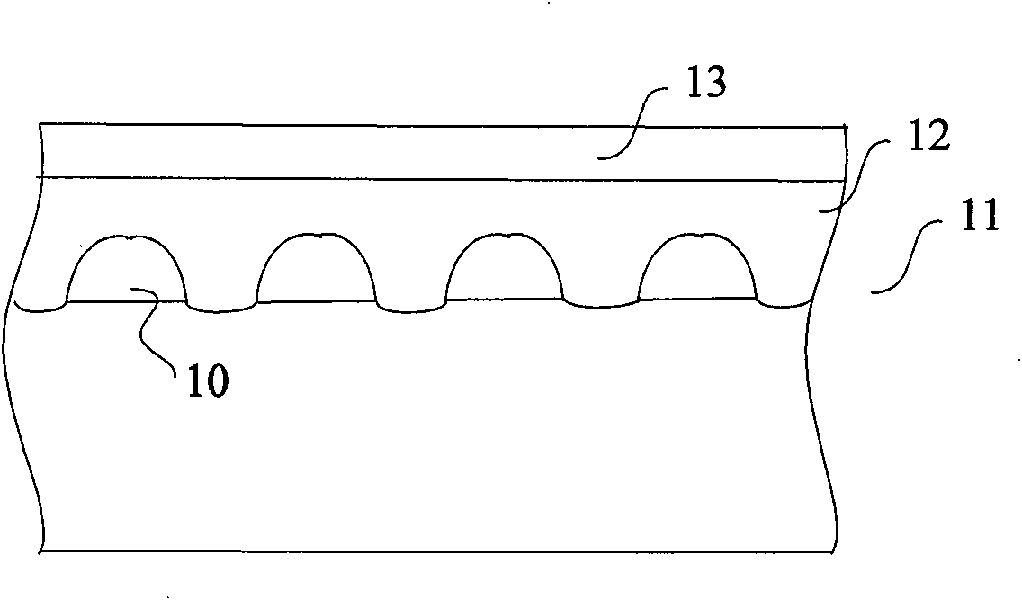
[0042] refer to Figure 5A , provide an initial TEM detection sample 51, the initial TEM detection sample 51 includes a Polymer mask 50; obtain the initial TEM detection sample 51 after dicing the wafer. .

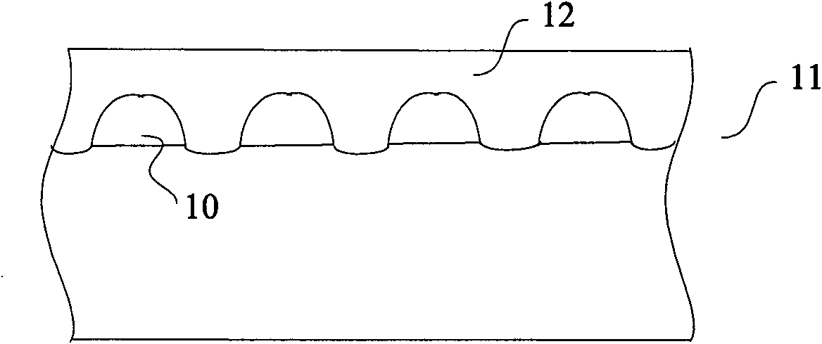
[0043] refer to Figure 5B , depositing a barrier layer 52 on the initial TEM detection sample 51;

[0044] In this embodiment, a Pt layer with a thickness greater than 20 nanometers is deposited as the barrier layer 52 by using PVD technology, and the specific process conditions include: a DC voltage of 0.4 kV, a vacuum pressure of 6 pascals, and a sample distance of 30 mm. represents the distance from the initial TEM detection sample 51 to the Pt target, and the Pt target is used to sputter Pt particles to form the barrier layer 52 on the initial TEM detection sample 51 . Based on the above process conditions, tho...


PUM

PropertyMeasurementUnit
Thicknessaaaaaaaaaa

Abstract

The invention provides a method for preparing a transmission electron microscope (TEM) detecting sample wafer to improve the quality of the TEM detecting sample wafer and further reducing the error of TEM detecting. The method comprises the following steps: providing an initial TEM detecting sample wafer; depositing a barrier layer on the TEM detecting sample wafer; depositing an electron-beam auxiliary layer on the barrier layer; and depositing an ion-beam auxiliary layer on the electron-beam auxiliary layer.

Description

technical field [0001] The invention relates to the fields of semiconductor manufacturing and material analysis, in particular to a preparation method of a transmission electron microscope (TEM, Transmission Electron Microscope) detection sample. Background technique [0002] The ion implantation process is a common semiconductor manufacturing process. Its principle is usually: based on a hard mask (hardmask), under certain process conditions, ions are implanted into the ion implantation region defined by the hard mask on the semiconductor substrate. ) is a commonly used hard mask material. [0003] With the development of technology, the feature size of semiconductor devices is gradually reduced, which puts forward higher and higher requirements for semiconductor manufacturing processes. For the ion implantation process, it is required that the profile (profile) and critical dimension (CD, Critical Dimension) of the hard mask meet the requirements accurately, otherwise the...

Claims


Application Information

Patent Timeline
IPC IPC(8): G01N1/28
Inventor 于会生胡建强赵燕丽芮志贤李明
Owner SEMICON MFG INT (SHANGHAI) CORP
Why Eureka
Try Eureka