Tunneling field-effect transistor and manufacturing method thereof

A technology of tunneling field effect and manufacturing method, which is applied in the direction of transistors, semiconductor/solid-state device manufacturing, semiconductor devices, etc., can solve the problems of reduced driving current and increased leakage current of tunneling transistors, and achieves increased driving current and reduced leakage current. Effect of small, reduced alignment requirements

Inactive Publication Date: 2012-09-05
FUDAN UNIV
View PDF0 Cites 0 Cited by
  • Summary
  • Abstract
  • Description
  • Claims
  • Application Information

AI Technical Summary

Problems solved by technology

However, while the leakage current is reduced, the driving current of the tunneling field effect transistor is also reduced. Therefore, the tunneling field effect transistor is still facing the challenge of how to increase the driving current.
[0004] Although the leakage current of the tunneling field effect transistor is lower than that of the traditional MOS tube, the leakage current of the tunneling transistor also increases with the shortening of the channel.

Method used


Image

  • Tunneling field-effect transistor and manufacturing method thereof
  • Tunneling field-effect transistor and manufacturing method thereof
  • Tunneling field-effect transistor and manufacturing method thereof

Examples


Embodiment Construction

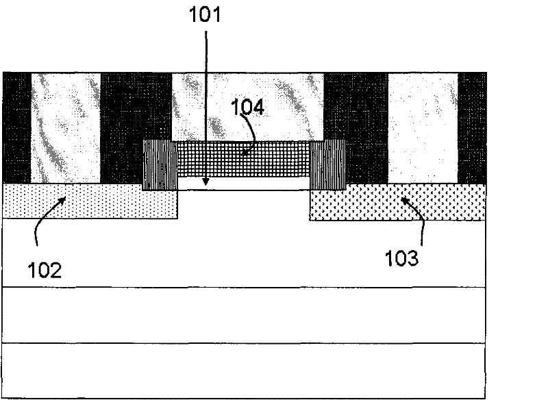
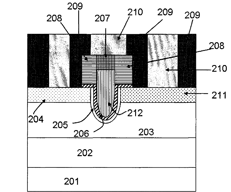
[0062] figure 2 It is an embodiment of the semiconductor recessed channel tunneling device disclosed in the present invention, and it is a cross-sectional view along the channel length direction of the device. This device has a gate stack region, a source region, a drain region, and a substrate region. The gate stack region is composed of an insulating layer 205, an insulating layer 206, a conductor layer 207 and a conductor layer 212. The insulating layer 205 is thermally oxidized grown or deposited silicon dioxide. The insulating layer 206 is a high dielectric constant medium. The conductive layer 207 is polysilicon, and the conductive layer 212 is a metal layer. The sidewall 208 of the gate stack area is an insulator such as Si 3 N 4 They insulate the gate conductor layer from the other conductor layers of the device. The doping type of the source doping region 211 is generally opposite to the doping type of the drain doping region 204, and is generally the same as the d...


PUM


Abstract

The invention belongs to the technical field of the semiconductor device, and particularly relates to a tunneling field-effect transistor and a manufacturing method thereof. The transistor comprises a source electrode, a drain electrode, a grid electrode and a substrate. The channel of the semiconductor device is indented towards the inside of the substrate, so as to reduce the leakage current and simultaneously drive the current to rise. The invention also discloses a manufacturing method of the semiconductor device. The semiconductor device manufactured by the invention has the advantages of low leakage current, high driving current, high degree of automation and the like. The invention can reduce the static power consumption of the integrated circuit and improve the integrated level thereof.

Description

Technical field [0001] The invention belongs to the technical field of semiconductor devices, and in particular relates to a tunneling field effect transistor with low power consumption using a recessed channel and a manufacturing method of such a device. Background technique [0002] Metal-oxide-silicon field effect transistors (MOSFET) are widely used in various electronic products. With the development of integrated circuit technology, the size of MOSFET is getting smaller and smaller, and the density of transistors on a unit array is getting higher and higher. The ensuing short channel effect has become more obvious. How to reduce the power consumption of portable devices has become a research hotspot in the field of semiconductor technology. Today's integrated circuit device technology node is around 50nm, and the leakage current between the source and drain of the MOSFET increases rapidly as the channel length shrinks. Especially when the channel length drops below 30nm,...

Claims


Application Information

Patent Timeline
Patent Type & Authority Patents(China)
IPC IPC(8): H01L29/78H01L29/10H01L29/49H01L21/336H01L27/088
Inventor 王鹏飞臧松干孙清清张卫
Owner FUDAN UNIV
Why Eureka
Try Eureka