Circuit and method for driving resistive random access memory to realize multi-valued storage

A technology of resistance conversion and driving resistance, which is applied in the direction of static memory, digital memory information, information storage, etc., and can solve the problem of low resistance of devices

A technology of resistance conversion and driving resistance, which is applied in the direction of static memory, digital memory information, information storage, etc., and can solve the problem of low resistance of devices

CN101783170AActive Publication Date: 2010-07-21INST OF MICROELECTRONICS CHINESE ACAD OF SCI

Image

  • Circuit and method for driving resistive random access memory to realize multi-valued storage
  • Circuit and method for driving resistive random access memory to realize multi-valued storage
  • Circuit and method for driving resistive random access memory to realize multi-valued storage

Examples


Embodiment Construction

[0017] In order to make the object, technical solution and advantages of the present invention clearer, the present invention will be described in further detail below in conjunction with specific embodiments and with reference to the accompanying drawings.

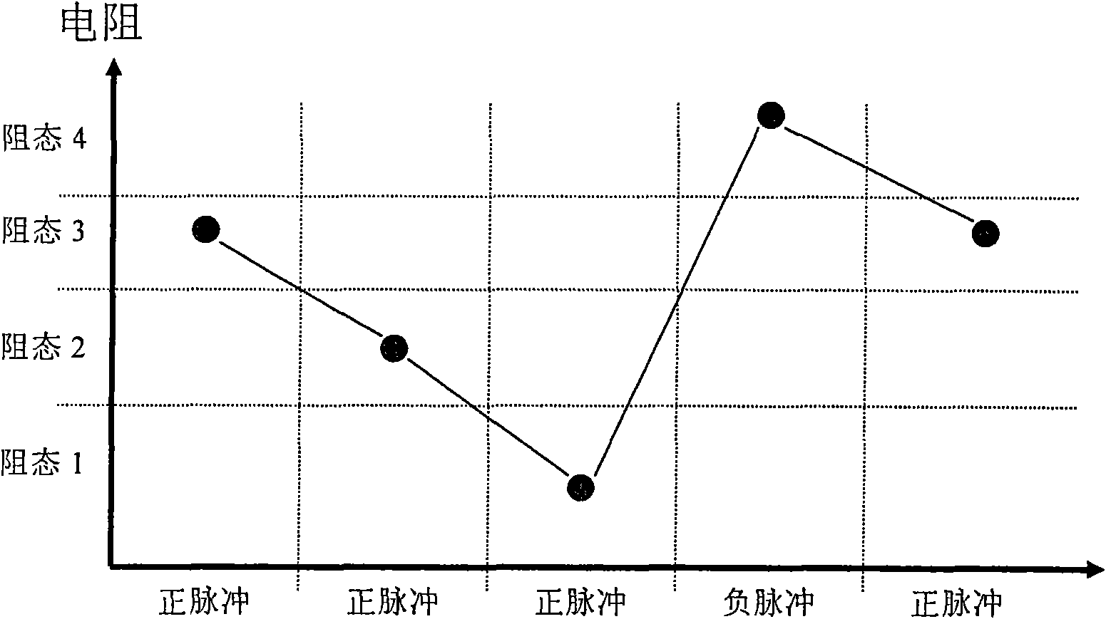
[0018] The invention provides a method for using capacitance storage energy to drive a resistance transition memory to perform state conversion and realize multi-value storage. The basic principle is to use capacitors with different electric energies as the excitation source to drive the resistance transition memory to undergo resistance transition, because the electric excitation amount of the resistance transition memory is different, so that the resistance transition state of the resistance transition memory is also different. , thus realizing multi-valued storage.

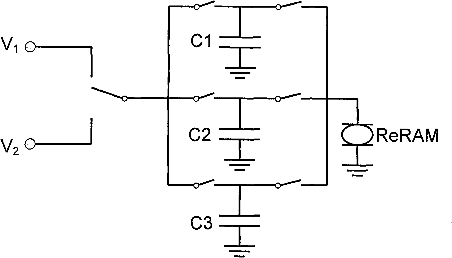
[0019] The circuit provided by the present invention for realizing multi-value storage by using a capacitance-driven resistance transition memory is compo...


PUM


Abstract

The invention discloses a circuit and a method for driving a resistive random access memory to realize multi-valued storage by using a capacitor. The circuit consists of a plurality of capacitors which are used for storing electric energy and have different capacitances, a plurality of voltage sources, the resistive random access memory, and a switching circuit, wherein the capacitors are connected to the voltage sources and the resistive random access memory through the switching circuit. The method comprises the following steps of: charging the capacitors having different capacitances to make the capacitors have the same voltage, or charging the capacitors having the same capacitance to make the capacitors have different voltages so as to make the capacitors store different electric energy; and then driving the resistive random access memory by using the capacitors having different electrical energy as signal excitation sources, and changing the resistance state of the resistive random access memory so as to make the resistive random access memory have different resistance states and realize the multi-valued storage. By using the circuit and the method, the multi-valued storage is realized by using a simple circuit to drive the resistive random access memory, and storage with a higher density in the same area is realized.

Description

technical field [0001] The invention relates to the technical field of microelectronic devices and memory, in particular to a circuit and method for realizing multi-value storage by using capacitance-driven resistance transition memory. Background technique [0002] The explosive growth of the consumer electronics market has led to the rapid growth of the non-volatile semiconductor memory (currently represented by flash memory), and it is expected that its total market value will soon exceed that of DRAM. However, conventional nonvolatile memory based on floating gate structures is encountering increasing difficulties in size reduction. This is mainly because the floating gate memory realizes the recording of information by storing or erasing charges in the polysilicon floating gate, thereby changing the threshold voltage of the MOS transistor. In order to store charges in the floating gate for more than 10 years, the thickness of the tunnel oxide layer cannot be excessivel...

Claims


Application Information

Patent Timeline
21 Jul 2010
Publication
CN101783170A
IPC
G11C11/56
CPC
G11C11/5685; G11C11/24; G11C13/0007; G11C11/56; G11C13/0002
Inventors
刘明; 张森