Semiconductor laser glue solidification device and application method thereof

A technology of glue curing and application method, applied in the field of laser applications, can solve the problems of high cost, low energy utilization rate, insufficient efficiency, etc., and achieve the effects of simple operation, fast heating and curing, and high energy utilization rate

Inactive Publication Date: 2010-07-28
WUHAN LINGYUN PHOTOELECTRONICS SYST
View PDF0 Cites 6 Cited by
  • Summary
  • Abstract
  • Description
  • Claims
  • Application Information

AI Technical Summary

Problems solved by technology

[0003] The purpose of the present invention is to provide a semiconductor laser glue curing device and application method to solve the problems in the above-mentioned prior art, such as low energy utilization rate, insufficient efficiency and high cost.

Method used


Image

  • Semiconductor laser glue solidification device and application method thereof
  • Semiconductor laser glue solidification device and application method thereof
  • Semiconductor laser glue solidification device and application method thereof

Examples


Embodiment Construction

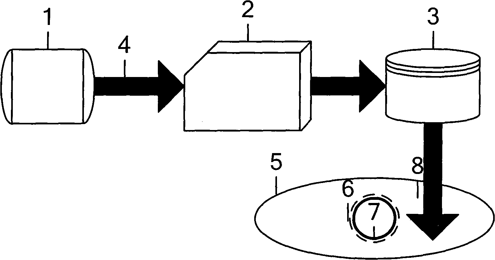
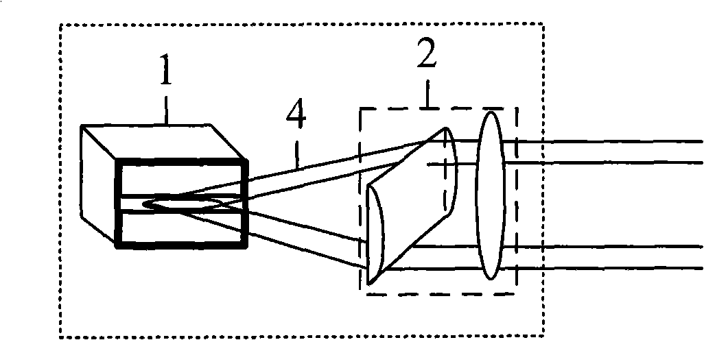
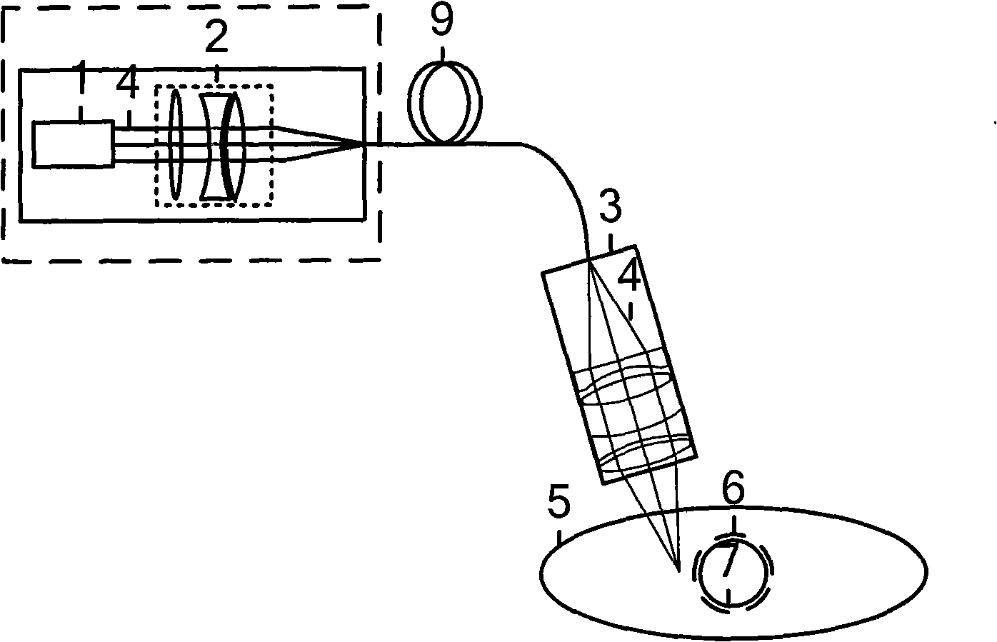
[0029] A semiconductor laser glue curing device and application method involved in the present invention, its technical scheme is combined with the attached Figures 1 to 7 The details are as follows:

[0030] Laser source of the present invention is produced by semiconductor laser diode 1 (taking center wavelength 980nm as light beam 4), and diode 1 can be the Bar bar that single tube or is made up of many diode single tubes; The light beam 4 that semiconductor laser diode sends, through optical shaping system 2 Shaping, collimation or focusing for transmission, the transmission mode is free space beam transmission or coupling into the energy transmission fiber 9 (the fiber length is 3m, the core diameter is 0.2mm, and the numerical aperture is 0.22) for transmission; then the transmitted laser beam 4 Reshape and focus through the optical collimation or focusing system 3; the optical collimation or focusing system 3 is composed of a single lens or multiple lenses, and both si...


PUM


Abstract

The invention relates to a semiconductor laser glue solidification device and an application method thereof. The device comprises a semiconductor laser light source, an optical beam shaping system, an optical beam transmission system, an optical beam scanning system, an optical focusing system, and the like. The application method comprises the following steps of generating the laser light source through a semiconductor laser diode, carrying out the shaping transmission on the semiconductor laser light source by adopting the optical beam shaping system and the optical beam transmission system, focusing the semiconductor laser light source to the appropriate spot size and working position through the optical focusing system, and irradiating a workpiece or glue so that the temperature of the glue rises rapidly and the glue is solidified rapidly. The invention can carry out partial or fixed-point heating on the workpiece, has the advantages of rapid solidification, low cost, high energy utilization ratio, and the like and can be widely applied to the field of heating solidification of various glues.

Description

technical field [0001] The invention belongs to the field of laser applications, in particular to a semiconductor laser glue curing device and an application method, which are suitable for various glue heating and rapid curing applications. technical background [0002] Glue has a wide range of applications in various industries, especially heat curing glue. In order to make the glue solidify quickly and improve production efficiency, it is necessary to increase the ambient temperature for glue curing. The usual practice is to coat the prepared glue on the workpieces to be bonded, and then place the workpieces in an oven with a constant temperature for heating, so that the glue can be quickly cured to achieve the purpose of bonding the workpieces. However, the oven is generally large in size and consumes a lot of power, so the utilization rate of energy is low and the cost is high. In addition, because the entire workpiece is to be placed in the oven, the temperature of th...

Claims


Application Information

Patent Timeline
IPC IPC(8): G02B27/09
Inventor 王锋汪建华刘良清
Owner WUHAN LINGYUN PHOTOELECTRONICS SYST
Why Eureka
Try Eureka