Infrared touch device based on double-frequency parallel scanning

An infrared touch and infrared emission technology, applied in the input/output process of data processing, instruments, electrical digital data processing, etc., can solve the problems of hysteresis, pause, increase the complexity of software and hardware, and achieve easy debugging and low production cost. , the effect of simple hardware and software structure

Inactive Publication Date: 2010-07-28
深圳新山鹰互动技术有限公司
View PDF2 Cites 1 Cited by
  • Summary
  • Abstract
  • Description
  • Claims
  • Application Information

AI Technical Summary

Problems solved by technology

Patent application 200610037391.X provides a technical solution using multiple master-slave microcontrollers. Although it can realize functions such as fast scanning and anti-interference, the disadvantage of multi-processors is that it greatly increases the complexity of the software and hardware in the entire system. degree, increasing the design and manufacturing cost of the infrared touch device
The technical solution disclosed in the patent application 200610140874.2 adopts a method of tracking the touch object to shorten the time required for detecting the touch object. It only involves the change of the internal control software of the microcontroller system, so it hardly increases the complexity and complexity of the system hardware. However, since the tracking range adopts a specific algorithm, when the touch object moves fast, or suddenly moves quickly, it is often the case that the touch object cannot be tracked and the whole area needs to be re-scanned, resulting in pauses and hysteresis

Method used


Image

  • Infrared touch device based on double-frequency parallel scanning
  • Infrared touch device based on double-frequency parallel scanning
  • Infrared touch device based on double-frequency parallel scanning

Examples


Embodiment Construction

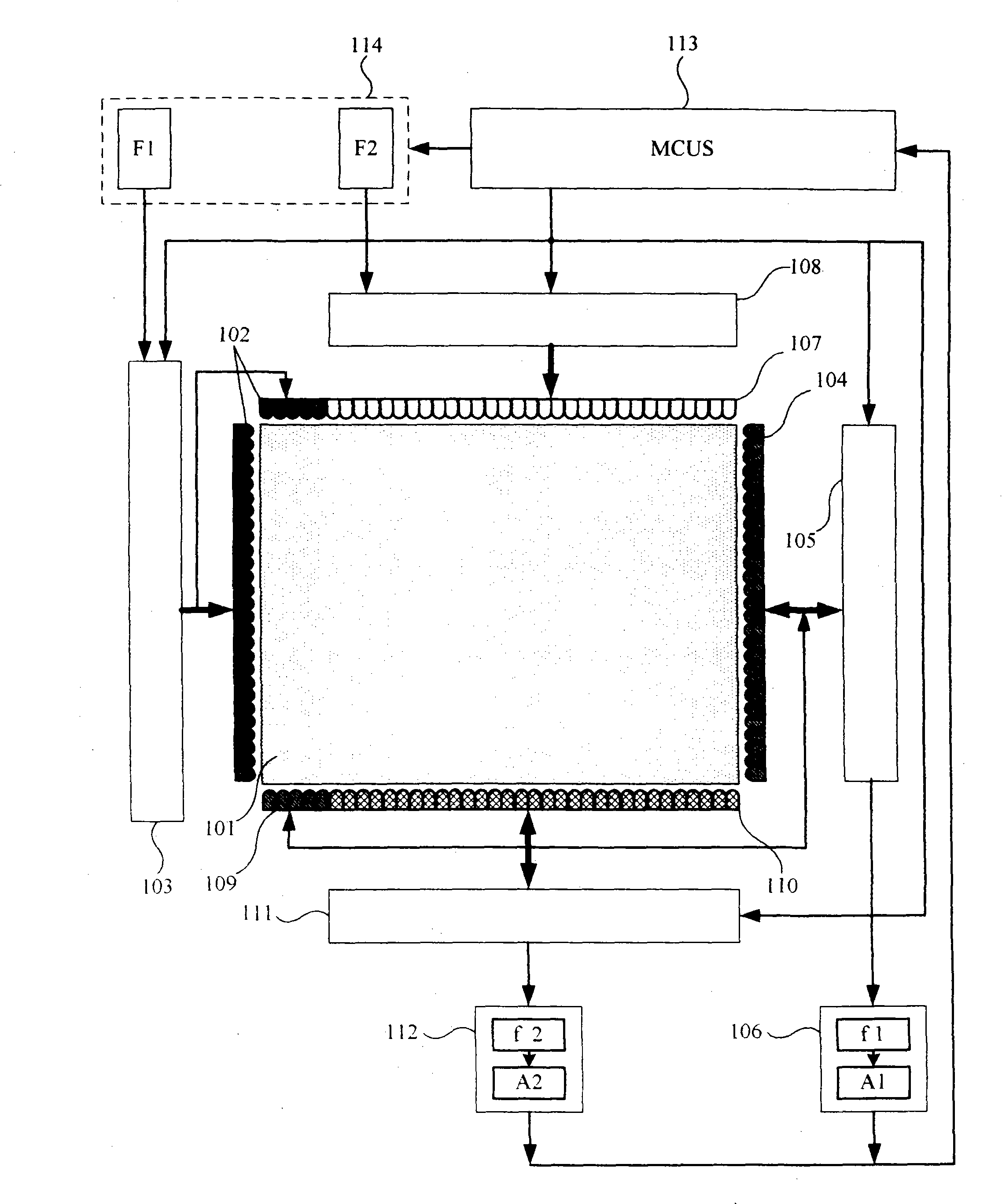
[0015] The basic embodiments of the present invention will be described below in conjunction with the accompanying drawings. Because the technical solution involved in the present invention is about the content of the circuit part for transmitting and receiving infrared signals, the specific mechanical structure of the infrared touch device (infrared touch screen) will not be given in the embodiment.

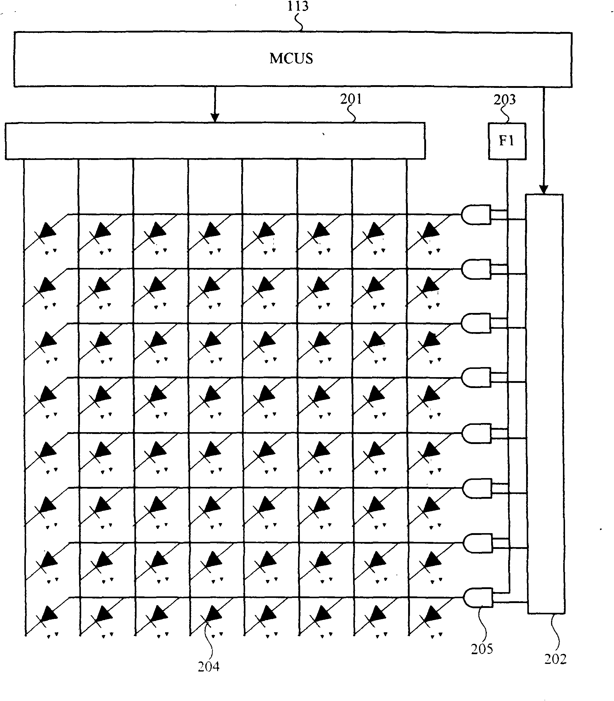
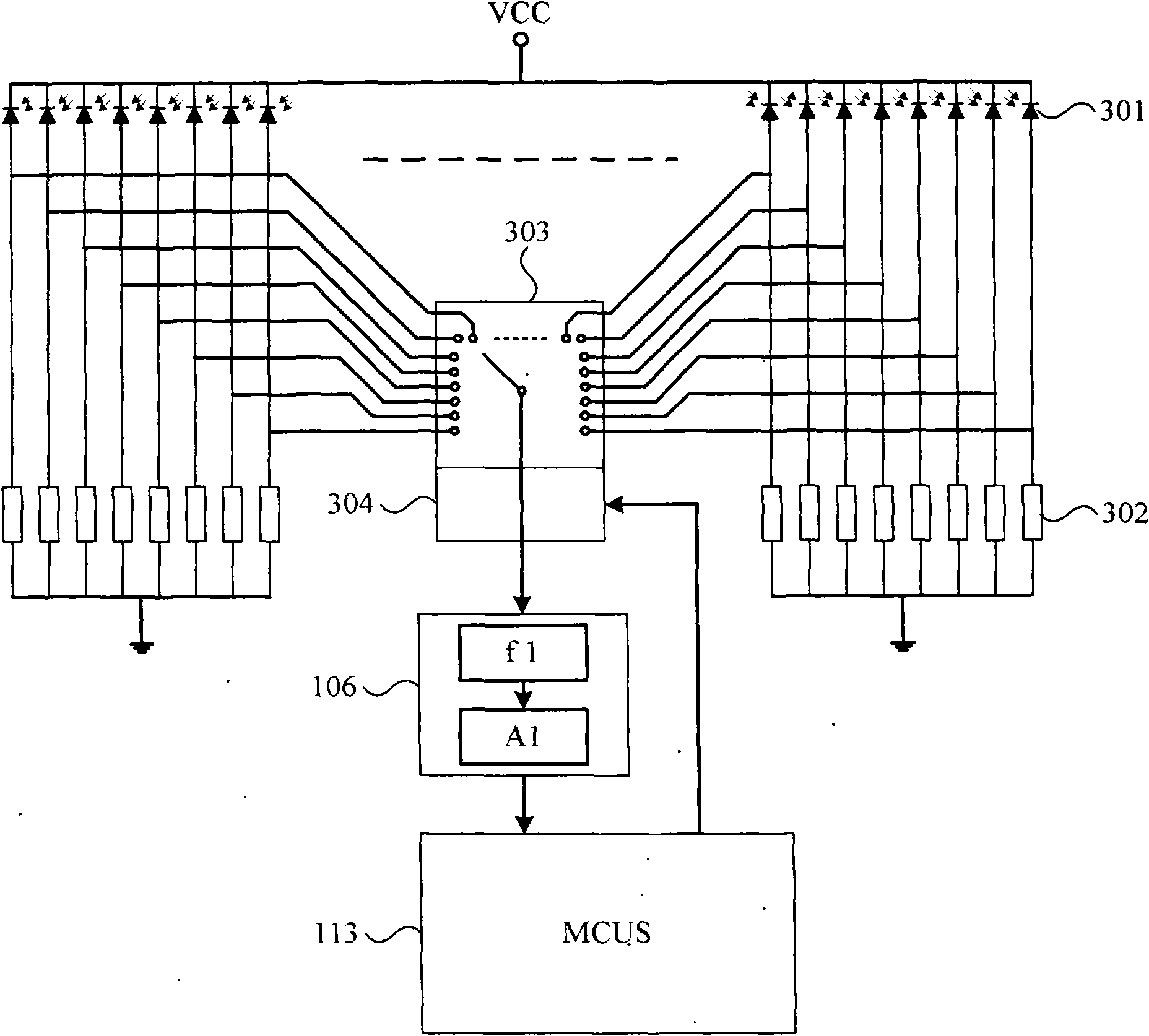
[0016] figure 1 It is a schematic diagram of the overall circuit structure of the infrared touch device of the present invention. Compared with the basic mechanism of the existing infrared touch device, there are two biggest differences in this figure: first, the infrared emitting tube and the receiving tube are divided into two independent groups, which are respectively connected with two infrared emitting drive modules and two Two infrared receiving gating modules are connected; secondly, a dual-frequency carrier frequency source 114 is included in the touch device, which inc...


PUM


Abstract

The invention provides an infrared touch device based on double-channel parallel scanning. The infrared touch device comprises two groups of paired infrared emitters and receivers and the corresponding driving and selecting modules, wherein each group comprises a driving module and a selecting module; the two groups of modules are subjected to synchronous control and operation by connecting the modules with the I / O (input / output) terminal of a micro-controller system; the infrared touch device further comprises two carrier generators having different frequencies, and the two carrier generators are respectively connected with the carrier inputting terminals of two groups of transmitting modules; and the infrared touch device further comprises two filter / amplifier circuits, and the transmission band of each filter circuit respectively corresponds to two output frequencies of the carrier generators. The two groups of paired infrared emitters and receivers in the invention can simultaneously scan the area to be detected, increase the scanning rate by one time at most and avoid the mutual interference in the modulation of different carriers. Therefore, the invention is particularly applicable to large infrared touch devices, has the advantages of simple software / hardware structure, low production cost, simple adjustment and the like and is suitable for industrialized production.

Description

technical field [0001] The invention relates to an infrared touch device, which belongs to the technical field of computer human-computer interaction, in particular to the technical field of touch point detection and scanning for an infrared touch device. Background technique [0002] The main structure and principle of the existing infrared touch device (that is, the infrared touch screen in general sense) is to install several pairs of infrared emitting and receiving tubes on the frame, and then use the microcontroller system inside the touch device through the I / O port to Control the driving module for driving the infrared emitting tube and the gating module for gating the infrared receiving tube, drive and gating each pair of infrared emitting and receiving tubes in a certain order, and complete the vertical and horizontal scanning of the touch surface. Then by detecting which pair of emitting and receiving tubes is blocked, the position of the touch object on the displa...

Claims


Application Information

Patent Timeline
IPC IPC(8): G06F3/042
Inventor 肖衣鉴
Owner 深圳新山鹰互动技术有限公司
Why Eureka
Try Eureka