Method for preparing multilayer raised compound film

A composite film layer and film layer technology, which is applied in the direction of manufacturing microstructure devices, microstructure technology, microstructure devices, etc., to achieve the effects of improving preparation speed, reducing errors, and reducing difficulty

Active Publication Date: 2011-09-28
INST OF OPTICS & ELECTRONICS - CHINESE ACAD OF SCI
View PDF0 Cites 0 Cited by
  • Summary
  • Abstract
  • Description
  • Claims
  • Application Information

AI Technical Summary

Problems solved by technology

[0006] In summary, so far, there is no simple process suitable for direct deposition of multi-layer non-uniform thickness film processing method on the substrate.

Method used


Image

  • Method for preparing multilayer raised compound film
  • Method for preparing multilayer raised compound film
  • Method for preparing multilayer raised compound film

Examples


Embodiment 1

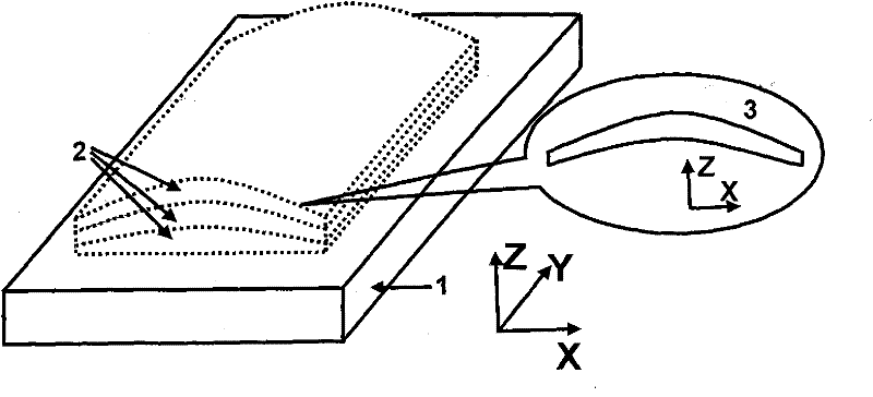
[0037] Embodiment 1 is to make a width of 8 microns and a length of 200 microns by the method of the present invention, which is composed of the first and third layers of silver and the second layer of silicon dioxide embossed structure film alternately. The manufacturing process is as follows:

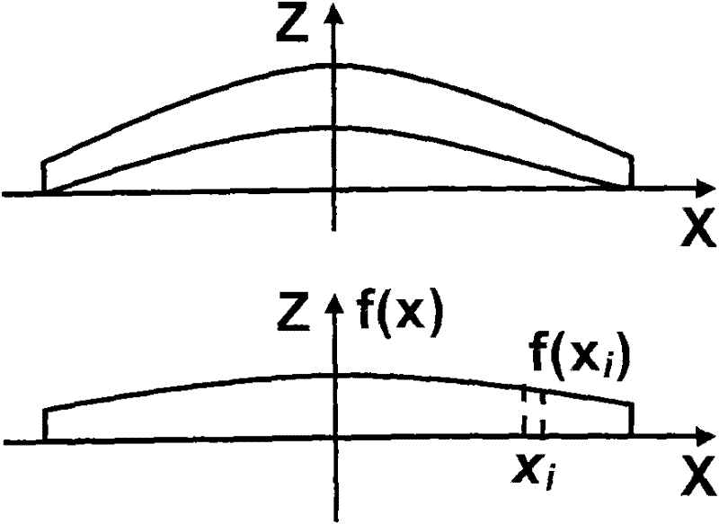
[0038] (1) As shown in Figure 1, the thickness distribution function of the film layer can be obtained by subtracting the function of the upper interface of any film layer of the super lens to be prepared by subtracting the function of the lower interface, so that the thickness of each film layer is obtained Distribution function;

[0039] Let the upper interface function of the i-th layer be f i (x), (i=1, 2, 3), where x is the moving direction of the mask, and the function of the interface on the substrate is f 0 (x)=0; the lower interface of the i-th film layer is the upper interface of the i-1th film layer, so the lower interface function of the i-th film layer and the upper inte...

Embodiment 2

[0047] Embodiment 2 is to make a SiO with a width of 20 microns and a length of 300 microns by the method of the present invention. 2 The two-layer optical lens composed of GaN and its production process is as follows:

[0048] (1) Subtracting its lower interface function from the upper interface function of any film layer of the super lens to be prepared can obtain the thickness distribution function of the film layer, so that the thickness distribution function of each layer film layer is obtained;

[0049] Let the upper interface function of the i-th layer be f i (x), (i=1, 2), where x is the moving direction of the mask, and the function of the interface on the substrate is f 0 (x)=0; the lower interface of the i-th film layer is the upper interface of the i-1th film layer, so the lower interface function of the i-th film layer and the upper interface function f of the i-1-th film layer i-1 (x) are equal;

[0050] Then the thickness distribution function g of the i-th f...


PUM

PropertyMeasurementUnit
widthaaaaaaaaaa
thicknessaaaaaaaaaa
thicknessaaaaaaaaaa

Abstract

The invention relates to a method for preparing a multilayer raised compound film and is characterized in that slits for passing deposited particles are manufactured on a mask; the slits of the mask are moved in the process of film material deposition to enable deposition areas to move on a substrate; the thickness of the film deposited in each area is controlled through controlling the time of deposition in each area of the substrate to condition the distribution of the thickness of the film; and the multilayer film with different film material and thickness distributions is continuously deposited in the same area of the substrate to obtain the multilayer raised compound film. The invention has the advantage of wide application prospect in the preparation of micro / nano raised structures.

Description

technical field [0001] The invention relates to a method for manufacturing a non-uniform thickness film, in particular to a method for preparing a micro / nano-scale multi-layer relief structure composite film layer based on the principle of a moving mask and the principle of directional deposition. technical background [0002] Micro / nano components, especially micro / nano optical components, have great application potential in scientific research, military, civil and other fields, for example, in the production of various SPPs components, optical data storage, super-resolution imaging, SPPs nanolithography etc. The preparation of micro / nano components containing multi-layer relief structure composite film layers is a difficult research point. Existing manufacturing methods can etch a single-layer relief structure film layer or deposit multiple film layers with uniform thickness, but it is difficult to prepare multi-layer relief structure composite film layers with non-unifor...

Claims


Application Information

Patent Timeline
Patent Type & Authority Patents(China)
IPC IPC(8): C23C14/22B81C1/00B82B3/00
Inventor 罗先刚王长涛冯沁刘凯鹏刘玲潘丽刘尧邢卉方亮
Owner INST OF OPTICS & ELECTRONICS - CHINESE ACAD OF SCI
Why Eureka
Try Eureka