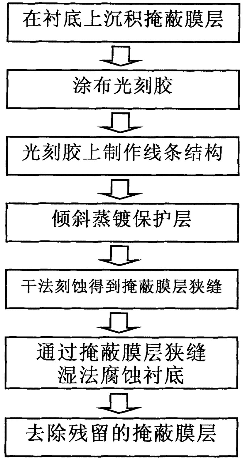
Method for fabricating smei-cylindrical groove by shadow evaporation and wet etching
A semi-cylindrical, wet etching technology, which is applied in vacuum evaporation plating, sputtering plating, ion implantation plating, etc., can solve the problems of high cost and processing area of only micron level, and reduce the production cost , the effect of efficient processing pathways
- Summary
- Abstract
- Description
- Claims
- Application Information
AI Technical Summary
Problems solved by technology
Method used
Image
Examples
Embodiment 1
[0043] Embodiment 1, making 5000 semi-cylindrical grooves with a diameter of 1 micron and a length of 20 mm, the specific manufacturing process is as follows:
[0044] (1) A quartz plate with a thickness of 365 microns is selected as the substrate; a 50nm thick chromium masking film is deposited on the substrate surface by magnetron sputtering technology, and a photoresist with a thickness of 100nm is coated on the chromium film.
[0045] (2) By exposing and developing, prepare such as on the photoresist image 3 The straight line structure shown; the straight line structure contains 5000 parallel straight lines with a width of 2 microns, a pitch of 1 micron, and a period, that is, the sum of the width and the pitch of 3 microns, and the length of the straight lines is 20 mm.
[0046](3) Gold is vapor-deposited obliquely at an angle of 45 degrees relative to the substrate plane. The thickness of the evaporated gold is 50 nm, and the edge of each photoresist line will form a re...
Embodiment 2
[0049] Embodiment 2, making 20,000 semi-cylindrical grooves with a diameter of 100 nm and a length of 5 mm, the specific manufacturing process is as follows:
[0050] (1) Select a K9 glass sheet with a thickness of 500 microns as the substrate; use magnetron sputtering technology to deposit a 20nm thick silicon masking film layer on the substrate surface, and coat a photoresist with a thickness of 50nm on the silicon film .
[0051] (2) By exposing and developing, prepare such as on the photoresist Figure 9 In the line structure shown, the period of the line structure is 500 nm, and the length of the line is 5 mm.
[0052] (3) Evaporate chromium at an angle of 20 degrees relative to the substrate plane, the thickness of the evaporated chromium is 30nm, and the edge of each photoresist line will form a region with a width of 20nm where no chromium is deposited as an evaporation material.
[0053] (4) Then dry-etch the silicon masking film layer with the vapor-deposition mate...
Embodiment 3
[0055] Embodiment 3, making 2 semi-cylindrical grooves with a diameter of 10 microns and a length of 500 microns, the specific manufacturing process is as follows:
[0056] (1) A quartz plate with a thickness of 1000 microns is selected as the substrate; a 400nm thick silicon masking film is deposited on the surface of the substrate by magnetron sputtering technology, and a photoresist with a thickness of 1000nm is coated on the silicon film.
[0057] (2) By exposing and developing, prepare such as on the photoresist Figure 15 The line structure shown; the line structure contains two photoresist lines with a width of 15 microns and a length of 500 microns. The distance between the two photoresist lines is 5 microns, and the rest of the substrate is removed. Engraving.
[0058] (3) Chromium is evaporated at an angle of 30 degrees relative to the substrate plane, the thickness of the evaporated chromium is 100nm, and a 500nm wide area without chromium deposited on the edge of ...
PUM
| Property | Measurement | Unit |
|---|---|---|
| diameter | aaaaa | aaaaa |
| thickness | aaaaa | aaaaa |
| thickness | aaaaa | aaaaa |
Abstract
Description
Claims
Application Information


