Amorphous silicon film solar cell film system, and film solar cell and manufacturing method thereof

A thin-film solar cell and amorphous silicon thin-film technology, which is applied in the direction of final product manufacturing, sustainable manufacturing/processing, circuits, etc., can solve the problems that restrict the application and development of thin-film solar cells, low photoelectric conversion rate, etc., and achieve the reduction of charged body Effect of recombination and retention, high photoelectric conversion rate, and increased drift speed

Inactive Publication Date: 2010-08-04
河南阿格斯新能源有限公司
View PDF6 Cites 1 Cited by
  • Summary
  • Abstract
  • Description
  • Claims
  • Application Information

AI Technical Summary

Problems solved by technology

However, the current thin-film photovoltaic modules generally have the problem of low photoelectric conversion rate, which is still around 6%, which restricts the application and development of thin-film solar cells.

Method used


Image

  • Amorphous silicon film solar cell film system, and film solar cell and manufacturing method thereof
  • Amorphous silicon film solar cell film system, and film solar cell and manufacturing method thereof
  • Amorphous silicon film solar cell film system, and film solar cell and manufacturing method thereof

Examples


Embodiment 1

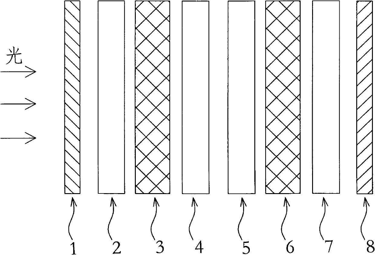
[0024] See figure 1 As shown, an amorphous silicon thin film solar cell film system is composed of the following parts:

[0025] heavily doped P + layer 1;

[0026] In heavily doped P + A first amorphous silicon p-i-n junction provided on one of the surfaces of layer 1, the first amorphous silicon p-i-n junction including p layer 2, i layer 3, and n layer 4;

[0027] A second amorphous silicon p-i-n junction arranged on the first amorphous silicon p-i-n junction, the second amorphous silicon p-i-n junction comprising a p layer 5, an i layer 6, and an n layer 7;

[0028] The heavily doped N arranged on the n layer 7 of the second amorphous silicon p-i-n junction + Layer 8.

Embodiment 2

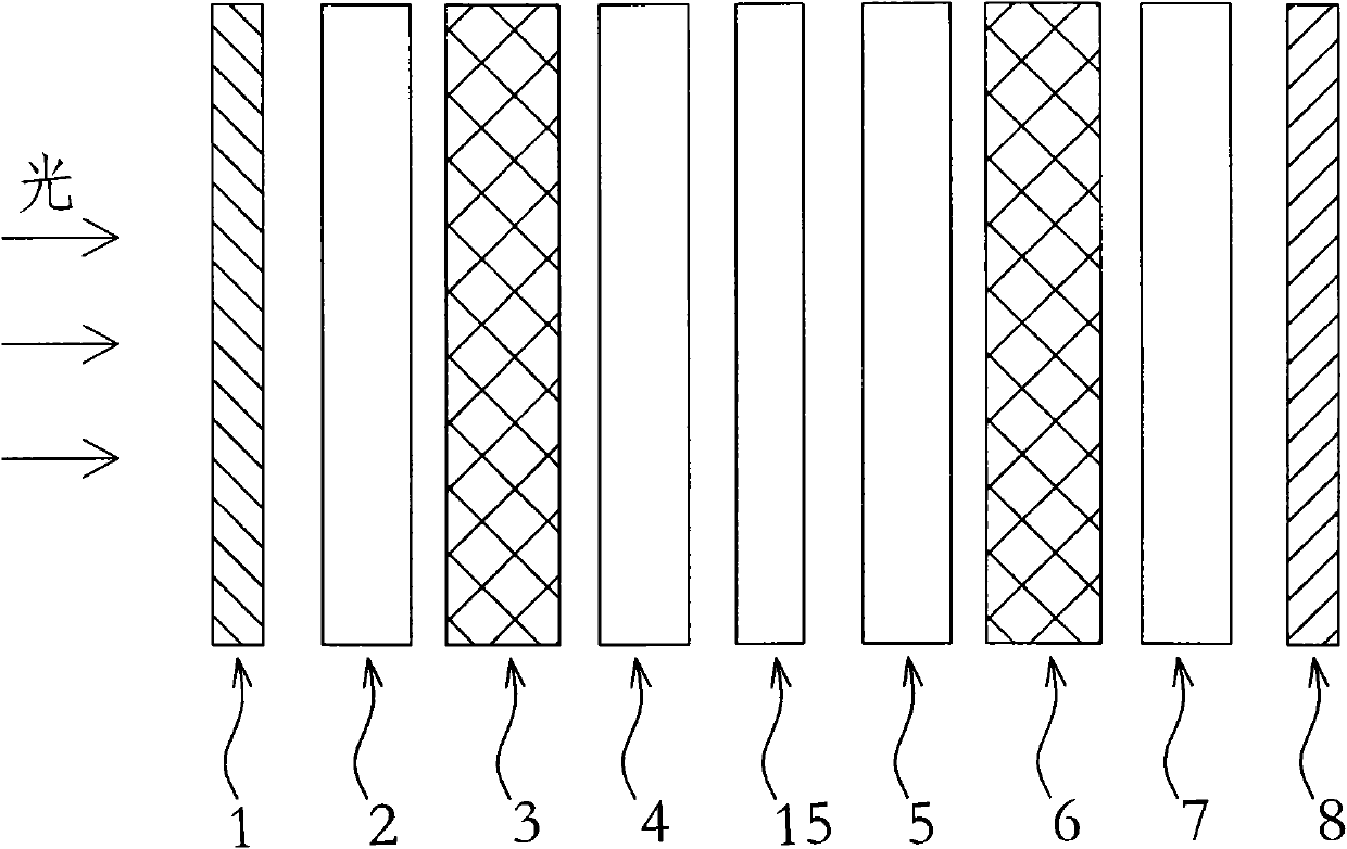
[0030] See figure 2 As shown, an amorphous silicon thin film solar cell film system is composed of the following parts:

[0031] heavily doped P + layer 1;

[0032] In heavily doped P + A first amorphous silicon p-i-n junction provided on one of the surfaces of layer 1, the first amorphous silicon p-i-n junction including p layer 2, i layer 3, and n layer 4;

[0033] A buffer layer 15 arranged on the n layer of the first amorphous silicon p-i-n junction, the buffer layer is a transparent conductive layer;

[0034] A second amorphous silicon p-i-n junction disposed on the buffer layer 15, the second amorphous silicon p-i-n junction comprising a p layer 5, an i layer 6, and an n layer 7;

[0035] The heavily doped N layer set on the n layer 7 of the second amorphous silicon p-i-n junction + Layer 8.

[0036] Adding the buffer layer 15 can increase the refraction times of light, thereby increasing the absorption ratio of light in the amorphous silicon thin film solar cell ...

Embodiment 3

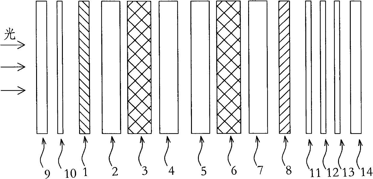
[0038] See image 3 As shown, a thin-film solar cell, the thin-film photovoltaic module of the thin-film solar cell is: along the direction of incident light, followed by a glass substrate 9, a transparent conductive film (TCO) 10 arranged on the glass substrate 9, and a transparent conductive film (TCO) 10 arranged on the transparent conductive P on membrane (TCO)10 + Layer 1, set in P + The first amorphous silicon p-i-n junction consisting of p-layer 2, i-layer 3, and n-layer 4 on layer 1, and the p-layer 5, i-layer 6, The second amorphous silicon p-i-n junction composed of n layer 7, the N disposed on the n layer 7 of the second amorphous silicon p-i-n junction + Layer 8, set in N +The ZnO layer 11 on the layer 8, the Al layer 12 arranged on the ZnO layer 11, the glued film (EVA) layer 13 arranged on the Al layer 12, the back plate glass 14 arranged on the glued film (EVA) layer 13, After heating, lamination and packaging, a thin film solar cell is produced.


PUM

PropertyMeasurementUnit
thicknessaaaaaaaaaa
thicknessaaaaaaaaaa

Abstract

The invention discloses an amorphous silicon film solar cell film system, which comprises a double-junction layer p-i-n/p-i-n formed by superposing a first amorphous p-i-n junction and a second amorphous p-i-n junction, wherein a p-type amorphous silicon layer of the second amorphous p-i-n junction is arranged on an n-type amorphous silicon layer of the first amorphous p-i-n junction, a p-type amorphous silicon layer of the first amorphous p-i-n junction is provided with a heavily-doped P+layer, an n-type amorphous silicon layer of the second amorphous p-i-n junction is provided with a heavily-doped N+layer, and the film structure has a structure of P+/p-i-n/p-i-n/N+. The heavily-doped P+layer and N+layer have the effect of reducing compounding and retaining properties of charged body, and simultaneously increase shift velocity of electric holes and electrons in semiconductor due to the reduction of twisting degree of an electric field in an i layer. The amorphous silicon film solar cell film system according to the invention has high photoelectric conversion rate and low cost, and the film solar cell manufactured according to the invention has the photoelectric conversion rate up to 7.5%.

Description

technical field [0001] The invention relates to an amorphous silicon thin-film solar cell film system and a thin-film solar cell, and at the same time relates to a manufacturing method of the thin-film solar cell, which belongs to the technical field of photovoltaic solar cells. Background technique [0002] With the tension and shortage of energy in the world, people pay more and more attention to the development of new energy, especially the development and utilization of green energy led by solar energy. Solar energy has been widely concerned and favored for its unique advantages such as no pollution, no geographical restrictions, and all-weather utilization. [0003] Based on maturity, reliability, low cost, ease of use in combination with other thin-film photovoltaic materials, and the ability to improve the process technology with the advancement of design and preparation methods, the thin-film photovoltaic module preparation technology for thin-film solar cells has be...

Claims


Application Information

Patent Timeline
Patent Type & Authority Applications(China)
IPC IPC(8): H01L31/042H01L31/0352H01L31/20
CPCY02E10/50Y02P70/50
Inventor 赵一辉
Owner 河南阿格斯新能源有限公司
Why Eureka
Try Eureka