Method for preparing back point contact structure of crystalline silicon solar cell

A contact structure, solar cell technology, applied in circuits, electrical components, semiconductor devices, etc., can solve problems such as harsh power requirements, low production efficiency, distorted substrate silicon wafer lattice structure, etc. low cost effect

Inactive Publication Date: 2010-08-11
上海太阳能电池研究与发展中心
View PDF3 Cites 2 Cited by
  • Summary
  • Abstract
  • Description
  • Claims
  • Application Information

AI Technical Summary

Problems solved by technology

For the passivation film prepared on the back of silicon solar cells, there are actually two issues to be considered: one is that the passivation film and the aluminum film on the back electrode form a highly reflective structure, which absorbs the near-infrared rays in the solar spectrum that have not been absorbed by the silicon chip. The radiation in the area is reflected back to the inside of the silicon wafer to improve the utilization of the incident spectrum; secondly, the passivation film cannot completely cover the back surface, and it is necessary to reserve a point contact structure in which the metal electrode that collects carriers is in contact with the substrate silicon wafer
The disadvantage of this method of preparing point contact structures is that the lasers used are relatively expensive and the production efficiency is not high. At the same time, the power requirements are relatively strict during the laser ablation process. Excessive power will seriously distort the lattice structure of the substrate silicon wafer. compound center
[0005] Zhao Lei et al. proposed "a method for preparing localized back contacts of crystalline silicon cells" (Chinese Patent Publication No. CN101359702A), which realized a process without using lasers, but the alumina used could only achieve partial passivation, while alumina Difficult to achieve back reflection structure

Method used


Image

  • Method for preparing back point contact structure of crystalline silicon solar cell
  • Method for preparing back point contact structure of crystalline silicon solar cell
  • Method for preparing back point contact structure of crystalline silicon solar cell

Examples


Embodiment Construction

[0023] Below in conjunction with accompanying drawing, specific implementation method of the present invention is described in further detail:

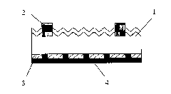
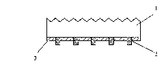
[0024] Such as figure 1 As shown, the upper surface of a crystalline silicon solar cell is a cell substrate 1 with a textured structure and a metal grid line 2 on the upper surface, and a passivation film 3 and an aluminum back electrode 4 are deposited on the back surface.

[0025] The preparation process of the back point contact structure of the crystalline silicon solar cell involved in the present invention is as follows:

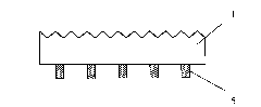
[0026] 1. According to the required crystalline silicon solar cell structure, determine the style of the cell back point contact structure, that is, the density of the point array and the size of the conductive contact point. The size of the contact point is usually 0.1-0.2mm, and the dot pitch is about 2mm, and the stencil for screen printing is made according to this pattern.

[0027] 2. Print the dot arra...


PUM


Abstract

The invention discloses a method for preparing a back point contact structure of a crystalline silicon solar cell, which specifically comprises the following steps of: carrying out screen printing on a prepared suede structure and the back surface of a P-N junction washed sample for preparing a photoetching glue point array; preparing a SiO2 passive film by using a vacuum film coating or PECVD (Plasma Enhanced Chemical Vapor Deposition) method and removing the photoetching glue point array by an alkali solution to form a back point contact structure. After an aluminum electrode is prepared on a substrate with the structure, the collection and the guide of current carriers are realized in the point array position. The preparation method has the advantages of changing a method for forming a back point contact structure array pattern by laser ablation into a screen printing method, having low cost, being suitable for mass production, and also having no obvious injury on the silicon substrate. Meanwhile, a SiO2 film with a thickness of 155 nm in the back surface position can form highest reflection in a near-infrared diffusion state with the interface position of the aluminum back electrode, thereby improving the conversion efficiency of the crystalline silicon cell.

Description

technical field [0001] The invention relates to a crystalline silicon solar photovoltaic cell, in particular to a preparation method for a back point contact structure of a crystalline silicon solar cell. technical background [0002] Solar power generation is one of the clean energy technologies that has developed very rapidly in recent years. According to statistics, the global output of solar cells in 2008 was 7.9GW, an increase of 85% compared with 2007. Nevertheless, compared with traditional thermal power, due to the high cost of various types of solar cells, the on-grid electricity price remains high, and solar power generation still does not have obvious price competitiveness. bottleneck. How to reduce the cost of solar power generation is one of the most concerned topics in the industry. [0003] Among all current solar cell products, crystalline silicon (including monocrystalline silicon and polycrystalline silicon) cells occupy about 90% of the market share. A...

Claims


Application Information

Patent Timeline
IPC IPC(8): H01L31/18
CPCY02P70/50
Inventor 王懿喆周呈悦马小凤梅伟芳
Owner 上海太阳能电池研究与发展中心
Why Eureka
Try Eureka