Trench type metal-oxide semiconductor device and manufacture method thereof

A technology of oxide semiconductor and manufacturing method, applied in semiconductor/solid-state device manufacturing, semiconductor device, electrical components and other directions, can solve the problems of increasing manufacturing cost, increasing the process complexity of metal oxide semiconductor components, etc., to improve efficiency, The effect of reducing the gate capacitance value and reducing the switching loss

Inactive Publication Date: 2010-08-18
NIKO SEMICON
View PDF0 Cites 7 Cited by
  • Summary
  • Abstract
  • Description
  • Claims
  • Application Information

AI Technical Summary

Problems solved by technology

However, in order to reduce the capacitance value from the gate to the drain of the metal oxide semiconductor device, the complexity of the process of the metal oxide semiconductor device is often greatly increased, resulting in an increase in the production cost.

Method used


Image

  • Trench type metal-oxide semiconductor device and manufacture method thereof
  • Trench type metal-oxide semiconductor device and manufacture method thereof
  • Trench type metal-oxide semiconductor device and manufacture method thereof

Examples


Embodiment Construction

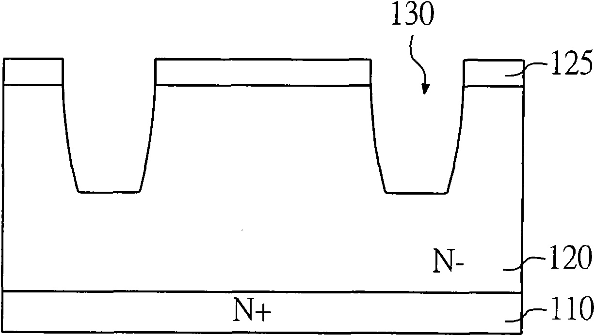
[0036] Figure 1A to Figure 1E The first embodiment of the manufacturing method of the trench metal oxide semiconductor device of the present invention is shown. Such as Figure 1A As shown, a substrate 110 is first provided, and an epitaxial layer 120 is formed on the substrate 110. Subsequently, a photoresist pattern layer 125 is fabricated on the upper surface of the epitaxial layer 120D to define the position of the gate channel 130. Next, the epitaxial layer 120 is etched through the photoresist pattern layer 125 to form at least one gate channel 130 in the epitaxial layer 120.

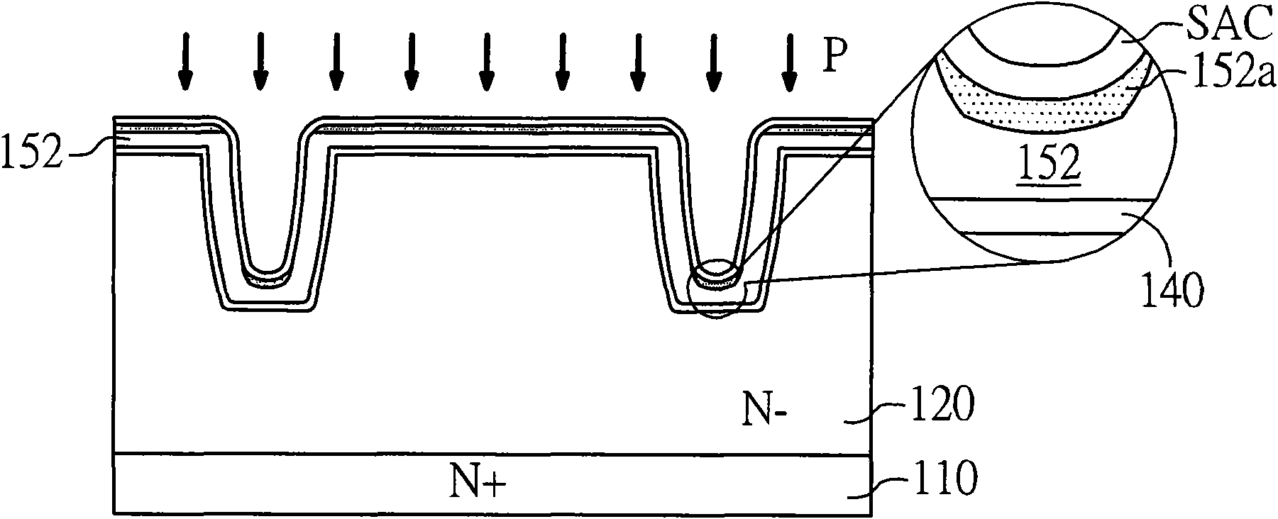
[0037] Then like Figure 1B As shown, the photoresist pattern layer 125 is removed, and a gate dielectric layer 140 is formed on the inner wall of the gate channel 130. The gate dielectric layer 140 may be made of silicon oxide or silicon nitride. In terms of the manufacturing process, the gate dielectric layer 140 made of silicon oxide can be formed on the exposed surface of the epitaxial layer 12...


PUM


Abstract

The invention relates to a manufacture method of a trench type metal-oxide semiconductor device. On a grid dielectric layer, a first polycrystalline silicon layer is deposited along the inner wall of a grid trench. Then, a first conductivity type dopant is implanted to the first polycrystalline silicon layer located at the bottom of the grid trench. Subsequently, a second polycrystalline silicon layer doped with a second conductivity type dopant is deposited to cover the first polycrystalline silicon layer. Subsequently, a high-temperature process is applied to enable the dopants in the firstpolycrystalline silicon layer and the second polycrystalline silicon layer to diffuse, and thereby, a first conductivity type first doping area and a second conductivity type second doping area whichare arranged at the bottom of the grid trench are formed.

Description

Technical field [0001] The invention relates to a channel type metal oxide semiconductor device and a manufacturing method thereof, in particular to a channel type metal oxide semiconductor device with low gate capacitance (Cgd) and a manufacturing method thereof. Background technique [0002] Compared with the traditional planar metal oxide semiconductor device, the current flow is along the direction parallel to the surface of the substrate. The channel metal oxide semiconductor device sets the gate in the channel to change the channel of the metal oxide semiconductor device. Position so that the current flow of the metal oxide semiconductor device is perpendicular to the substrate. Therefore, the size of the component can be reduced, the enthusiasm of the component can be improved, and the manufacturing cost can be reduced. Common metal oxide semiconductor devices on the market include metal oxide semiconductor field effect transistors (MOSFET), insulated gate diode transisto...

Claims


Application Information

Patent Timeline
Patent Type & Authority Applications(China)
IPC IPC(8): H01L21/8234H01L27/088H01L29/423H01L29/92H01L29/78
Inventor 许修文
Owner NIKO SEMICON
Why Eureka
Try Eureka