

Preparation method of thin film transistor based on induced longitudinal crystallization polycrystalline silicon
A polysilicon thin film and thin film transistor technology, which is applied in the manufacture of semiconductor/solid state devices, electrical components, circuits, etc., can solve the problems of unstable performance of polysilicon thin films and high leakage current, so as to reduce current and gate-induced drain leakage current, The effect of reducing the residual concentration
Inactive Publication Date: 2010-08-25
GUANGDONG SINODISPLAY TECH
View PDF2 Cites 12 Cited by
- Summary
- Abstract
- Description
- Claims
- Application Information
AI Technical Summary
Problems solved by technology
When the MILC method is used, the pure metal nickel deposited by evaporation is usually used as the induced film material, but the obtained polysilicon film contains more nickel residues, and the ratio of nickel / silicon is about 10 -3 The order of magnitude (IEEE Trans, Electron Devices, 48 (1655), 2001), this higher nickel residual concentration easily causes the unstable performance of the polysilicon thin film prepared, so that the off-state current (I off ) and gate-induced leakage current (GIDL) are higher
Method used
View moreImage
Smart ImageViewing Examples


Examples
preparation example Construction
Login to View More PUM
 Abstract
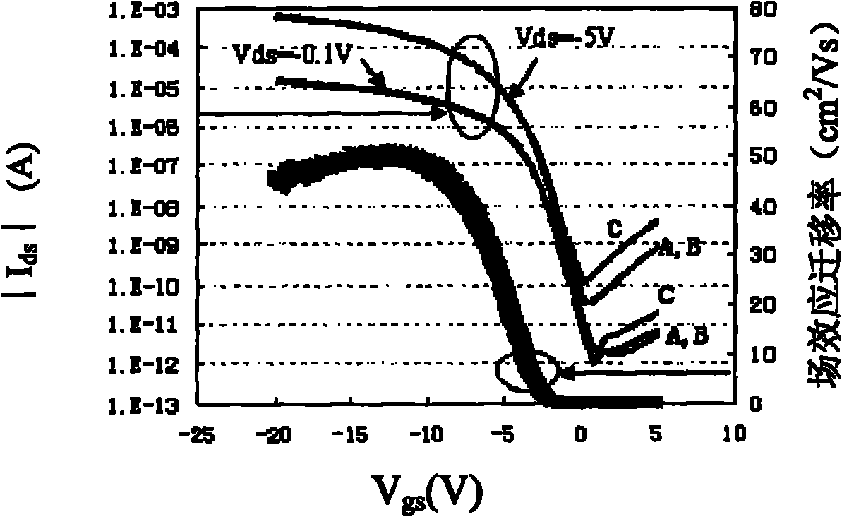
The invention provides a preparation method of a thin film transistor based on an induced longitudinal crystallization polycrystalline silicon film, which comprises the steps of: forming a noncrystalline silicon layer on a substate and forming an oxide layer; etching a groove on the oxide layer to expose the noncrystalline silicon layer; forming a nisiloy oxide film with thickness of 100nm on the exposed noncrystalline silicon layer and annealing for 1h at a temperature of 590 DEG C under an inert or protective gas environment; after finishing crystallization, removing residual nisiloy oxide and the oxide layer and forming an active island through photoetching; depositing 100nm of oxide layer; irradiating the surface of a sample by adopting pulse laser; finally, forming a source leakage electrode after ions are injected by using a grid insulation layer as the 100nm oxide layer and 280nm polycrystalline silicon as a grid electrode; and depositing a 500nm oxide layer to form a contact hole and a metal leading-out electrode. By adopting the method, close state current of the TFT and leakage current of a grid initiation leakage electrode are lowered.
Description
technical field The invention belongs to the field of thin film transistor preparation, in particular to a preparation method of a thin film transistor based on a laterally induced crystallization low temperature polysilicon thin film. Background technique Although most active-matrix liquid crystal displays (AM-LCDs) are still mostly composed of amorphous silicon (a-Si) thin-film transistors (TFTs), for active-matrix displays, polysilicon (p-Si) thin-film transistors can be used. Provides higher resolution and smaller pixels, and when using polysilicon TFTs, some driver circuits can also be integrated on the glass substrate. In addition, polysilicon TFTs are more stable than amorphous silicon TFTs in driving organic light-emitting diode displays (OLEDs), so low-cost, high-performance and more reliable low-temperature polysilicon (LTPS) processing techniques are required. Existing methods for obtaining polycrystalline silicon thin films mainly include solid state crystalliz...
Claims
Login to View More Application Information
Patent Timeline
 Patent Type & Authority Applications(China)
IPC IPC(8): H01L21/336H01L21/20
Inventor 赵淑云
Owner GUANGDONG SINODISPLAY TECH