Micro plane-type gas spark gap switch
A gas spark gap, planar technology, applied in the direction of spark gaps, spark gap parts, electrical components, etc., can solve the problems of inconvenient integration and integration, inconvenient practical application, long trigger time of switches, etc., to improve reliability and safety Resilience, increased strength and effect, shortened trigger time effects
- Summary
- Abstract
- Description
- Claims
- Application Information
AI Technical Summary
Problems solved by technology
Method used
Image
Examples
Embodiment 1
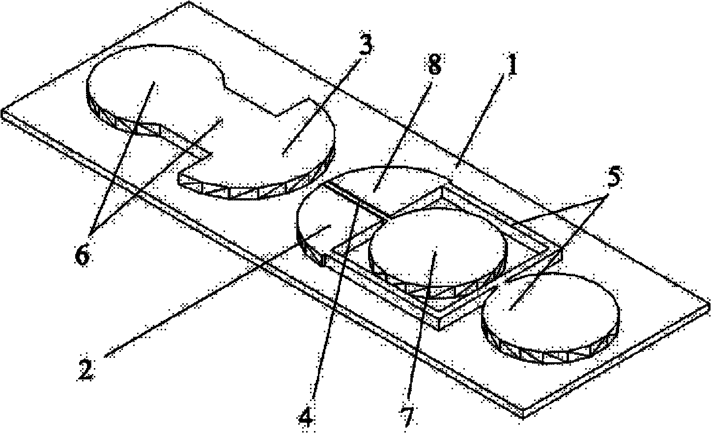
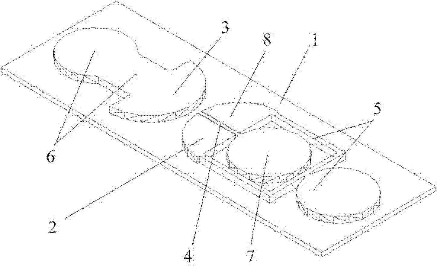
[0028] As shown in Figure 1, this embodiment includes: an insulating substrate 1, a first negative electrode 2, a second negative electrode 8, a positive electrode 3, a trigger electrode 4, a negative electrode connection unit 5, a positive electrode connection unit 6 and a trigger electrode The connection unit 7, wherein: the first negative electrode 2 and the second negative electrode 8, the positive electrode 3, the trigger electrode 4, the negative electrode connection unit 5, the positive electrode connection unit 6 and the trigger electrode connection unit 7 are all fixed on the insulating substrate 1 Above, the trigger electrode 4 is located between the first negative electrode 2 and the second negative electrode 8, the positive electrode connection unit 6 is connected to the positive electrode 3, and the negative electrode connection unit 5 is connected to the first negative electrode 2 and the second negative electrode 8 respectively, The trigger electrode connection u...
Embodiment 2
[0041] As shown in FIG. 4 , the difference between this embodiment and Embodiment 1 is that the insulating substrate 1 is a quartz substrate, and the shapes of the first negative electrode 2 , the second negative electrode 8 and the positive electrode 3 are all rectangular parallelepiped. Quartz substrate can improve the insulating effect of the substrate. The distance between the first negative electrode 2 and the second negative electrode 8 is 200 microns, and the dimensions of the two negative electrodes are: 1000 microns in length, 800 microns in width, and 200 microns in height, and are made of multiple stacked electroplating nickel or copper metals . The distance between the positive electrode 3 and the first negative electrode 2 and the second negative electrode 8 is 1500 microns, the size of the positive electrode 3 is: 2000 microns in length, 800 microns in width, and 200 microns in height. make.
[0042] This embodiment can reduce the damage and ablation of the fir...
Embodiment 3
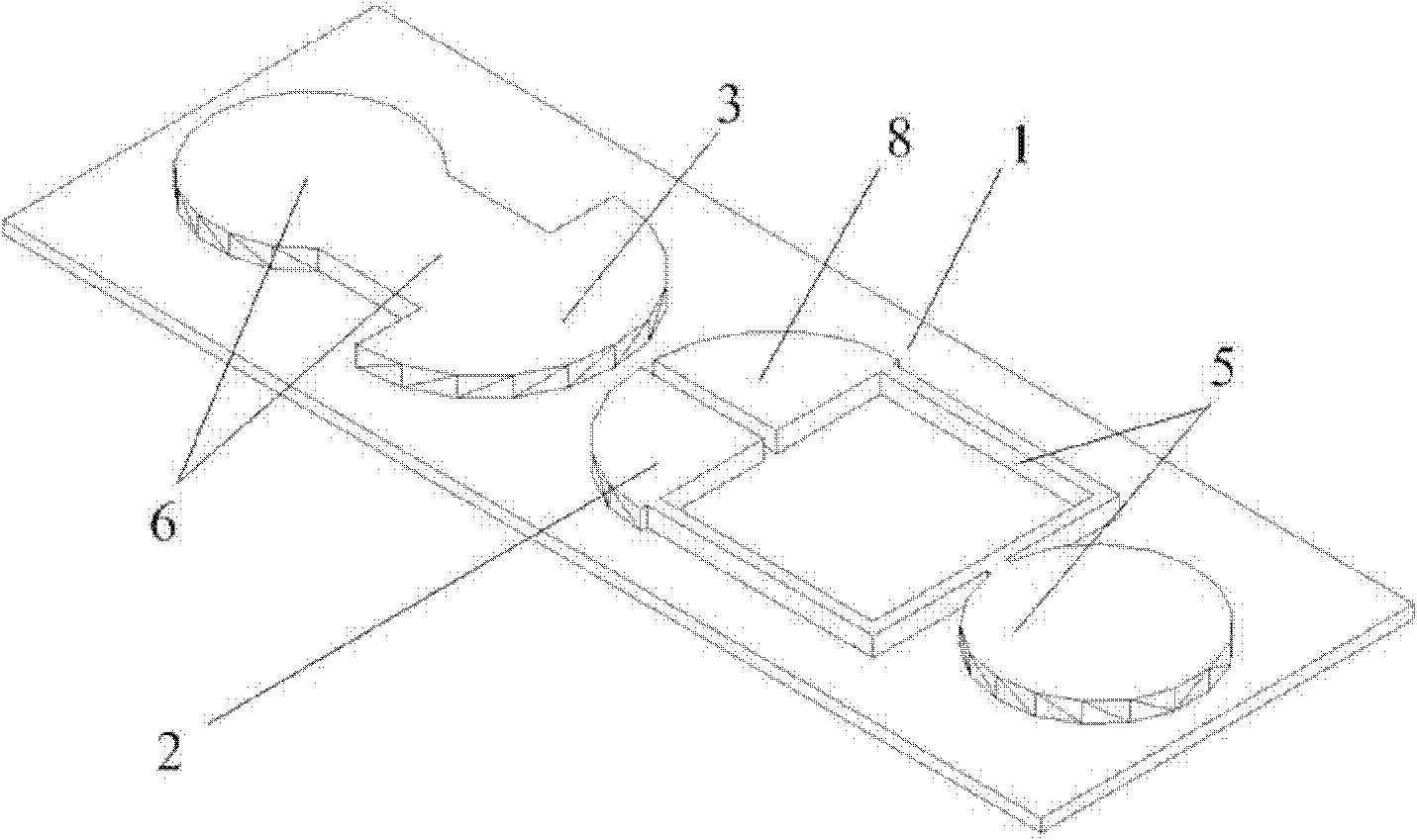
[0044] As shown in Figure 5, the difference between this embodiment and Embodiment 1 is that the trigger electrode 4 is located between the negative electrode 2 and the positive electrode 3, the distance between the first negative electrode 2 and the second negative electrode 8 is 100 microns, and the positive electrode 4 is located between the negative electrode 2 and the positive electrode 3. 3 is a semi-circular cylinder with a radius of 800 microns and a height of 100 microns, the distance between the first negative electrode 2 and the second negative electrode 8 is 800 microns, and it is made of multiple layers of electroplated nickel or copper metal. The distance between the trigger electrode 4 and the first negative electrode 2 and the second negative electrode 8 is 50 microns.
[0045] This embodiment can improve the spark discharge effect between the first negative electrode 2 , the second negative electrode 8 and the trigger electrode 4 , increase the number of electr...
PUM
| Property | Measurement | Unit |
|---|---|---|
| Spacing | aaaaa | aaaaa |
| Area | aaaaa | aaaaa |
| Height | aaaaa | aaaaa |
Abstract
Description
Claims
Application Information


