Method for machining PCB with step groove

A PCB board and processing technology technology, which is applied in the field of PCB board processing technology with stepped grooves, can solve problems such as easy delamination and peeling, poor welding, poor etching, etc., to reduce product scrapping, improve product quality, and increase contact area. Effect

Active Publication Date: 2012-07-04
SHENNAN CIRCUITS
View PDF0 Cites 0 Cited by
  • Summary
  • Abstract
  • Description
  • Claims
  • Application Information

AI Technical Summary

Problems solved by technology

[0014] 1. The area of ​​the step groove is directly connected to the electroplated copper and the copper of the base material. The steps of the step groove are all covered with copper skin. When the components are soldered here and reflowed at high temperature, the internal stress and water vapor of the substrate cannot be released, which makes the electroplating copper easy to be separated from the substrate. Poor bonding force of the base material is easy to be delaminated and peeled off, resulting in poor welding and affecting product reliability
[0015] 2. The existing PCB board processing technology has already milled out the through groove before electroplating. When processing the outer layer graphics and pasting dry film protection, due to the large hollow area in the middle step groove, the film is easy to wrinkle or cause the film to break, thus It is easy to cause defects such as poor etching, resulting in product scrapping and increasing costs

Method used


Image

  • Method for machining PCB with step groove
  • Method for machining PCB with step groove
  • Method for machining PCB with step groove

Examples


Embodiment Construction

[0035] In order to describe the technical content, structural features, achieved goals and effects of the present invention in detail, the following will be described in detail in conjunction with the embodiments and accompanying drawings.

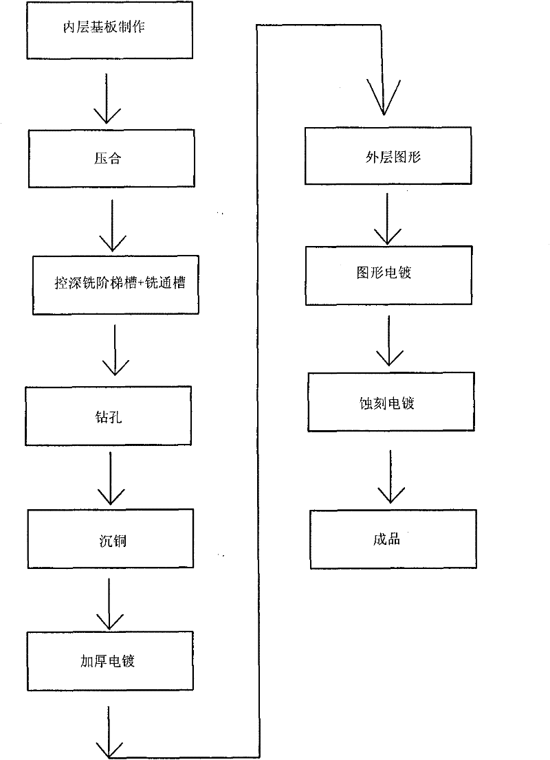
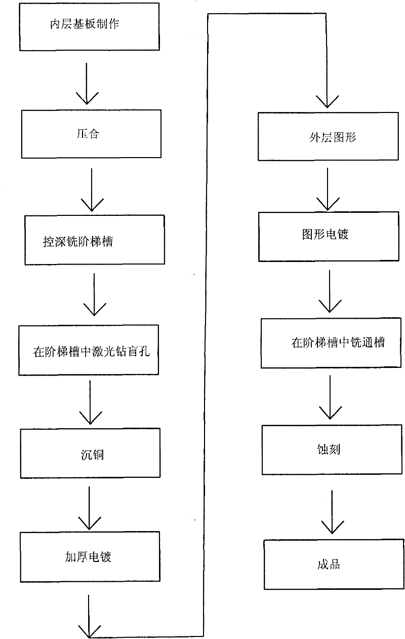
[0036] see image 3 and Figure 4 , the present invention has the PCB board processing method of step groove and comprises the following steps:

[0037] A. The production of PCB inner substrate;

[0038] B. Press the substrate to form a PCB board;

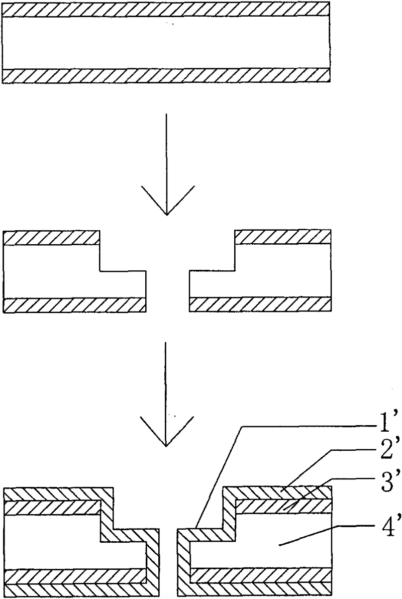
[0039] C. Mill a stepped groove 20 of a certain depth on the PCB formed after lamination;

[0040] D. Carry out laser drilling on the surface of the stepped groove 20, and drill a plurality of blind holes 21;

[0041] E, sinking copper on the surface of the PCB (including the surface of the stepped groove 20 and the two side walls of the blind hole 21);

[0042] F, carry out thickening electroplating to the PCB board after sinking copper in the step E;

[0043] G. Carry out outer layer gr...


PUM


Abstract

The invention discloses a method for machining a PCB with a step groove, which comprises the following steps: milling the step groove on the PCB formed after pressing; drilling a plurality of blind holes in the step groove by using laser; performing copper deposition electroplating on the surface of the PCB; performing pattern electroplating on the PCB after copper deposition; and milling a through groove on the surface of the step groove after the pattern electroplating. By designing the metallized laser blind holes on the surface of the step groove, the method for machining the PCB with thestep groove can effectively increase the contact area between electroplating copper and a base material, effectively enhance the bonding force between the electroplating copper and the base material,improve the quality of a product, and avoid the phenomenon of poor welding caused by layered peeling of the electroplating copper and the base material; and the through groove is milled after the pattern electroplating, so the board surface is flat when outer layer pattern machining is performed on the PCB, the film sticking effect is good, poor etching can be effectively improved, and the condition of product scrap is reduced.

Description

technical field [0001] The invention relates to a PCB board processing method with stepped grooves. Background technique [0002] Generally, stepped grooves are provided on the PCB board to accommodate electrical components, so as to prevent the electrical components from protruding out of the circuit board and occupying the external space. see figure 1 and figure 2 , the current PCB board processing method with metallized step grooves generally includes the following: [0003] A. The production of PCB inner substrate 4'; [0004] B. Press the substrate to form a PCB board; [0005] C. Mill a stepped groove with a certain depth, and drill a through groove to obtain a stepped groove 1'; [0006] D. Drilling; [0007] E. Carry out copper plating on the substrate copper 3' surface of the PCB board drilled with stepped grooves; [0008] F, the surface of the PCB board in the step E is carried out to thicken the electroplating of sinking copper, among the figure 2 ' is el...

Claims


Application Information

Patent Timeline
Patent Type & Authority Patents(China)
IPC IPC(8): H05K3/00H05K3/18
Inventor 王富成王彩霞许瑛钱文鲲韩雪川
Owner SHENNAN CIRCUITS
Why Eureka
Try Eureka