Piezoelectric crystal element
A technology of piezoelectric crystals and piezoelectric elements, applied in piezoelectric devices/electrostrictive devices, manufacturing/assembly of piezoelectric/electrostrictive devices, material selection for piezoelectric devices or electrostrictive devices, etc. , can solve the problems of low piezoelectric coefficient, not widely used, difficult to synthesize, etc.
- Summary
- Abstract
- Description
- Claims
- Application Information
AI Technical Summary
Problems solved by technology
Method used
Image
Examples
Embodiment 1
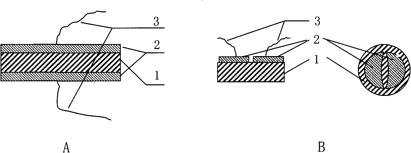
[0078] Using high-purity CaCO 3 、 Ta 2 o 5 、Al 2 o 3 , SiO 2 Raw materials, according to Ca: Ta: Al: Si = 3: 1: 3: 2 ingredients, after mixing, briquetting, high temperature sintering into polycrystalline materials, and then use the melt pulling method for crystal growth to obtain Ca 3 TaAl 3 Si 2 o 14 (CTAS) crystals. Orientate, cut, grind and polish the crystal, and process it into X-cut discs with a diameter of 9mm and a thickness of 0.35mm, and then coat Pt electrodes on both X surfaces, sinter at high temperature, and finally weld on the Pt electrodes The Pt lead is attached to complete the preparation of the CTAS high temperature piezoelectric crystal element.
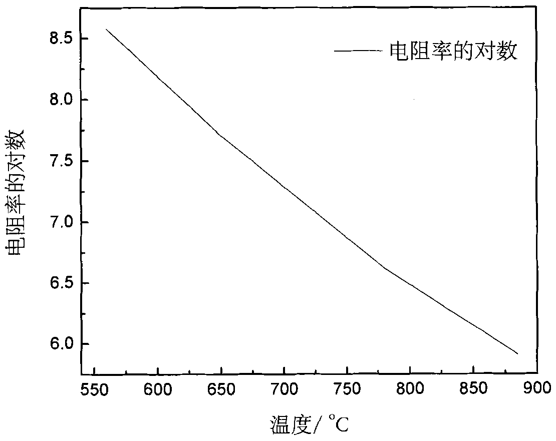
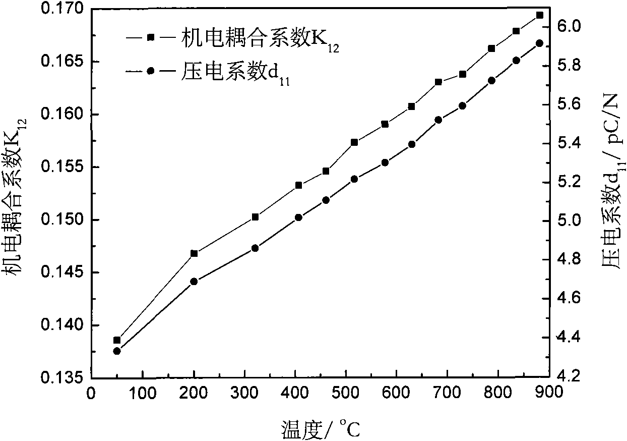
[0079] Then the CTAS high temperature piezoelectric crystal element is placed in a special high temperature furnace, the lead wire is connected with a special sample clamp, and the resistance in the high temperature range from room temperature to 900 °C is measured with a Keithley 2410 measuring instrume...
Embodiment 2
[0081] Using high-purity CaCO 3 , Nb 2 o 5 、Al 2 o 3 , SiO 2 Raw materials, according to Ca: Nb: Al: Si = 3: 1: 3: 2 ingredients, after mixing, briquetting, high temperature sintering into polycrystalline materials, and then use the melt pulling method for crystal growth to obtain Ca 3 NbAl 3 Si 2 o 14 crystals. The crystal is oriented, cut, ground, polished, processed into a Y-cut disc with a diameter of 9mm and a thickness of 0.35mm, and then coated with Pt electrodes on both Y surfaces, sintered in a high temperature environment, and finally welded on the Pt electrodes The Pt lead is attached to complete the preparation of the high temperature piezoelectric crystal element.
Embodiment 3
[0083] Using high-purity CaCO 3 , SrCO 3 、 Ta 2 o 5 、Al 2 o 3 , SiO 2 Raw materials, according to Ca: Sr: Ta: Al: Si = 2.9: 0.1: 1: 3: 2 ingredients, mixed, compacted, high-temperature sintered polycrystalline material, and then filled into the iridium crucible, put the crucible into In the cavity of the intermediate frequency induction heating crystal growth pulling furnace, the protective atmosphere is N 2 +0.5%O 2 . The specific growth process includes heating up the polycrystalline material for 3 hours until the polycrystalline material melts, and keeping the temperature for 4 hours to stabilize the melt; using X-direction seed crystals, and starting to pull and grow at about 50°C higher than the melting temperature; using a rotation speed of 15rpm, pulling The speed is 1 mm / h. At the end of the growth, the crystal is lifted from the melt, and the temperature is lowered at a rate of 100 ° C per hour, and Ca is obtained after cooling. 2.9 Sr 0.1 TaAl 3 Si 2 o ...
PUM
 Abstract
Description
Claims
Application Information


