Method for manufacturing high-thermal conductivity circuit board by hot-pressing method and high-thermal conductivity circuit board

A high thermal conductivity, circuit board technology, applied in the electrical field, can solve the problems of no further conduction of heat sink heat, damage to the electrical circuit of the circuit board, limited heat dissipation effect, etc., and achieve the effect of simple structure, good heat dissipation effect and low cost.

Inactive Publication Date: 2010-09-22
ZHUHAI BONTECH ELECTRIC TECH
View PDF8 Cites 16 Cited by
  • Summary
  • Abstract
  • Description
  • Claims
  • Application Information

AI Technical Summary

Problems solved by technology

[0004] However, the above-mentioned patented technology is only aimed at the installation of the heat sink on the circuit board after the electrical circuit has been completed, and its defects are: first, the process of installing the heat sink is an independent process after the circuit board is completed, which increases the workload; secondly, through When the die squeezes the heat sink, it may damage the electrical circuit on the circuit board
It can be said that the above-mentioned patented technology is more suitable for the installation of individual power devices, but not suitable for the installation of a large number of power devices with high density and array distribution.
In addition, the heat of the heat sink in the above-mentioned patented technology has no further conduction, and the heat dissipation effect is limited

Method used


Image

  • Method for manufacturing high-thermal conductivity circuit board by hot-pressing method and high-thermal conductivity circuit board
  • Method for manufacturing high-thermal conductivity circuit board by hot-pressing method and high-thermal conductivity circuit board
  • Method for manufacturing high-thermal conductivity circuit board by hot-pressing method and high-thermal conductivity circuit board

Examples


Embodiment 1

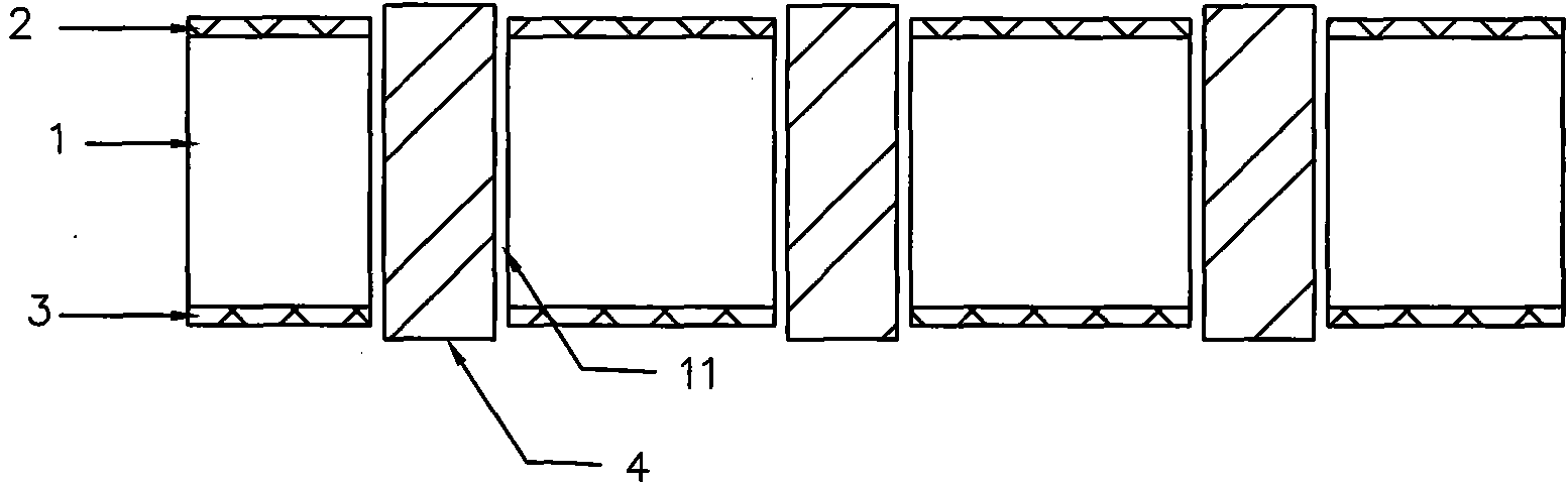
[0021] See Figure 1A-Figure 1D , the method for making a high thermal conductivity circuit board provided by this embodiment includes the following steps:

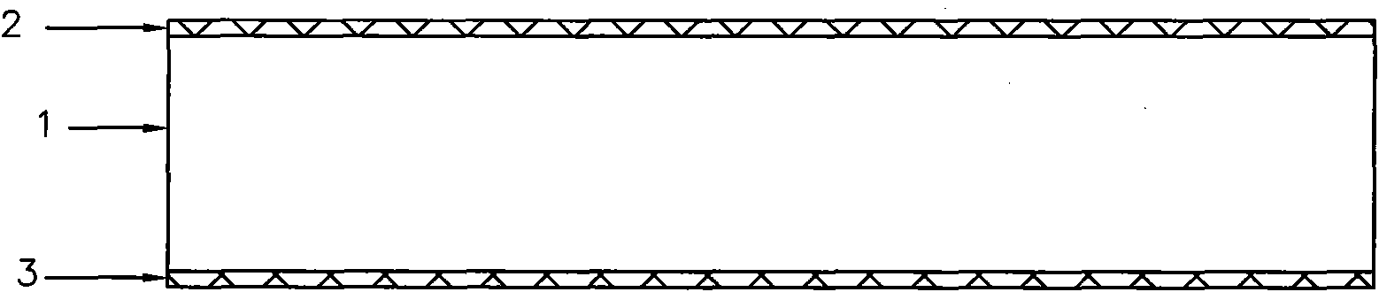
[0022] (1) Provide an insulating substrate layer 1 (which can be FR4 sheet or BT sheet), attach a metal conductive layer 2 on the upper surface of the insulating substrate layer 1, and attach a metal thermally conductive layer 3 on the lower surface, thereby forming a double-sided tape Metal layer plate; (2) drilling several through holes 11 on the double-sided metal layer plate; (3) manufacturing a number of metal heat conduction columns 4 matching with the through holes; (4) placing metal heat conduction columns 4 into the through holes 11 (5) Use a hot press to heat-press the metal heat-conducting column 4 so that it is assembled in the through hole 11. In this embodiment, the volume of the metal heat-conducting column 4 just fills the volume of the through-hole 11 after hot pressing; (6 ) to etch the excess metal laye...

Embodiment 1

[0024] The high thermal conductivity circuit board that embodiment 1 makes is as Figure 1D As shown, it includes an insulating base material layer 1, an electrical circuit layer (not shown in the figure, but well known to those skilled in the art), a metal heat conduction layer 3 and a metal heat conduction column 4, and the electrical circuit layer is arranged on the upper surface of the insulating base material layer 1 , the metal heat conduction layer 3 is arranged on the lower surface of the insulating base material layer 1, and the double-sided metal layer sheet has a through hole 11 at the preset heating element; the metal heat conduction column 4 is arranged in the through hole 11, and its upper end is used to communicate with the heat generating element. The pre-set heating element (not shown in the figure) is thermally conductively matched, and the lower end is thermally conductively matched with the metal heat conducting layer 3 .

Embodiment 2

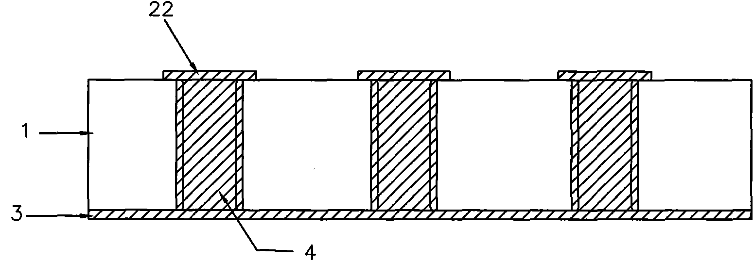
[0026] See Figure 2A-Figure 2E , the method for making a high thermal conductivity circuit board provided by this embodiment includes the following steps:

[0027] (1) Open some through holes 11 on the insulating substrate layer 1 (which can be FR4 sheet or BT sheet); (2) Make some metal heat conduction columns 4 that cooperate with the through holes; (3) Make the metal heat conduction columns 4 Put it into the through hole 11; (4) attach the metal conductive layer 2 on the upper surface of the insulating base material layer 1, and attach the metal heat conducting layer 3 on the lower surface, and hot press and cure; (5) on the insulating base material layer 1 The redundant metal layer is etched on the surface to form electrical connection lines and some pads 22 ( Figure 2D Only pads are shown in ); the method provided by this embodiment may further include step (6): selectively plating electrical connection lines and several pads, gold-plated, silver-plated, tin-sprayed or...


PUM


Abstract

The invention relates to a method for manufacturing a high-thermal conductivity circuit board and the high-thermal conductivity circuit board, which aim to solve the heat dissipation problem of heating elements on the circuit board. In the invention, by means of comprehensive consideration and overall arrangement of the implementation procedures of the high-thermal conductivity circuit board, the assembly procedures of a heat conducting column is integrated into the making process of the circuit board, which is implemented mainly as follows: before forming an electrical connecting line, the heat conducting column is assembled in a preset position of the circuit board; the method does not affect subsequent procedures and avoids reworking after the circuit board is formed; and a metal heat conducting layer can further dissipate heat on the heat conducting column, thus achieving better heat dissipation effect and having simple operation, simple structure and low cost.

Description

【Technical field】 [0001] The invention relates to a printed circuit board in the electrical field and a manufacturing method thereof. 【Background technique】 [0002] The power device heats up significantly during the working process. If the heat cannot be dissipated in time, the power device may be damaged, and even the entire electronic product may work abnormally. Taking LED lighting products as an example, a large number of LEDs are usually arranged intensively on the circuit board. When the LEDs work for a long time, the heat accumulation will shorten the life of the LEDs and make the product characteristics unstable. [0003] China Patent Application No. 200810241905.2 discloses a method for assembling a heat sink on a circuit board and a heat dissipation circuit substrate manufactured by the method. The method for assembling the heat sink comprises the following steps: making at least one through hole on the circuit board; making a heat sink matching the clearance of ...

Claims


Application Information

Patent Timeline
Patent Type & Authority Applications(China)
IPC IPC(8): H05K3/00H05K1/02H05K7/20H01L21/48H01L23/498
CPCH01L2924/0002
Inventor 孙百荣
Owner ZHUHAI BONTECH ELECTRIC TECH
Why Eureka
Try Eureka