Inductive component and method for manufacturing the same

A manufacturing method and component technology, which are applied in the field of chip inductor components and their manufacturing, can solve problems such as cracks in welding parts, and achieve the effects of increasing the number of stacks, improving practical reliability, and suppressing wire breakage.

Inactive Publication Date: 2014-04-02
PANASONIC CORP
View PDF6 Cites 2 Cited by
  • Summary
  • Abstract
  • Description
  • Claims
  • Application Information

AI Technical Summary

Problems solved by technology

Therefore, applying stress to the insulating material constituting the green body 25 may cause cracks in the welded portion

Method used


Image

  • Inductive component and method for manufacturing the same
  • Inductive component and method for manufacturing the same
  • Inductive component and method for manufacturing the same

Examples


Embodiment approach 1

[0024] Hereinafter, an inductance component and a method for manufacturing the same according to Embodiment 1 of the present invention will be described with reference to the drawings.

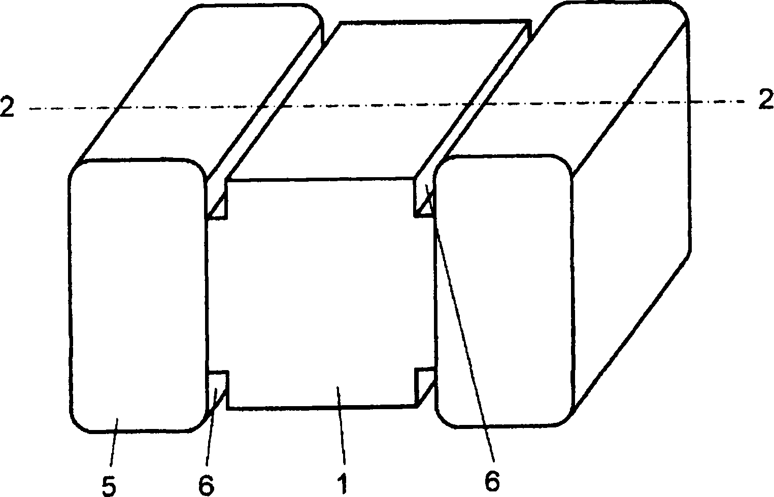
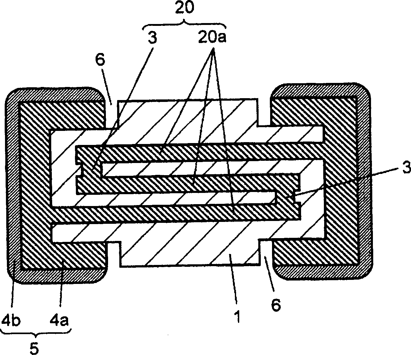
[0025] figure 1 It is a perspective view of the inductance component in Embodiment 1 of this invention. figure 2 Yes figure 1 Sectional view of part 2-2. exist figure 1 , figure 2 Among them, the inside of the body 1 made of an insulating resin obtained by curing a photosensitive resin is laminated using a plating technique and a photolithography technique so that the coil pattern 20a is formed into a spiral shape via the through electrodes 3 Thus, the coil portion 20 is formed.

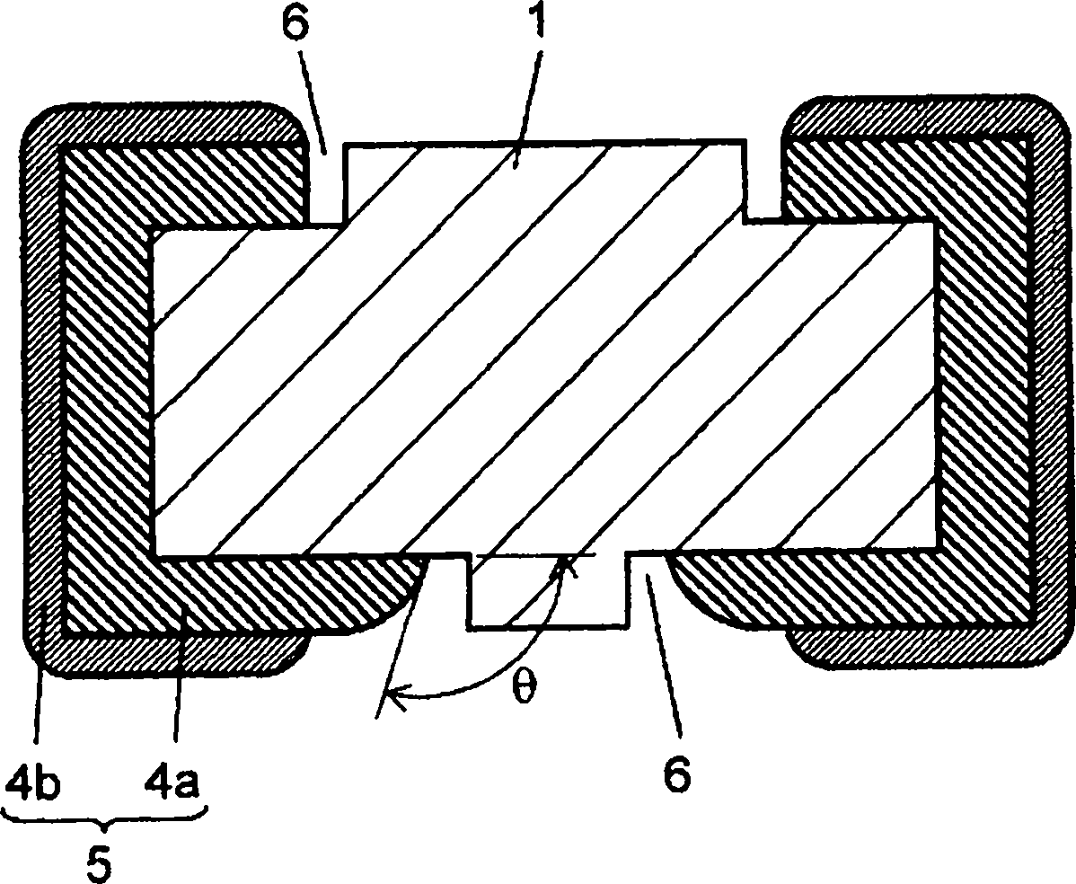
[0026] The through electrodes 3 correspond to the interlayer connection portions of the plurality of coil patterns 20a. The coil patterns 20a formed of multiple layers are connected in a spiral shape or a coil shape via the through electrodes 3 formed at predetermined positions. At this time, in order to ...


PUM

PropertyMeasurementUnit
elastic modulusaaaaaaaaaa

Abstract

An inductance component is disclosed. This inductance component includes base made of insulating material, coil section buried in base, and external electrode terminals electrically coupled to the ends of coil section. Stress buffering section is provided on the exposed interface between base and external electrode terminals, and this stress buffering section can ease the stress produced by the difference in thermal coefficients due to temperature changes. The foregoing structure thus allows improving the reliability of the inductance component with respect to a thermal shock.

Description

technical field [0001] The present invention relates to a chip-type inductor component used in electronic equipment such as mobile phones and a method for manufacturing the same. Background technique [0002] Conventionally, as such a chip-type inductor component, a ceramic electronic component obtained by sintering an electrode material having excellent conductivity such as silver or copper is formed inside a ceramic body by a printing technique. Figure 12 It is a cross-sectional view of a conventional inductor component. exist Figure 12 Among them, for the purpose of miniaturization and high precision, a blank 25 made of an insulating material, a coil portion 21 formed inside the blank using a plating technique and a photolithography technique, and a coil portion connected to the end of the coil portion 21 are used. The external electrode terminals 23 and 24 constitute a conventional inductance component. [0003] For these chip-type inductor components, miniaturization...

Claims


Application Information

Patent Timeline
Patent Type & Authority Patents(China)
IPC IPC(8): H01F37/00H01F41/04
CPCH01F41/041H01F17/0013Y10T29/49073
Inventor 山本宪一大庭美智央松谷伸哉
Owner PANASONIC CORP
Why Eureka
Try Eureka