Circuit board and method for manufacturing the same

A circuit substrate and circuit technology, applied in printed circuit manufacturing, printed circuits, printed circuits, etc., can solve problems such as damage to the conductivity of electrical wiring, and achieve the effect of preventing corrosion and excellent corrosion resistance.

Inactive Publication Date: 2010-09-29
PANASONIC CORP
View PDF3 Cites 8 Cited by
  • Summary
  • Abstract
  • Description
  • Claims
  • Application Information

AI Technical Summary

Problems solved by technology

[0004] Here, as described above, when the circuit 3 is formed from the copper plating layer 5, copper and its alloys have high conductivity, but they are corroded in normal environments to generate reactive oxides or sulfides, which may significantly damage the circuit. Conductivity of wiring

Method used


Image

  • Circuit board and method for manufacturing the same
  • Circuit board and method for manufacturing the same
  • Circuit board and method for manufacturing the same

Examples


Embodiment 1

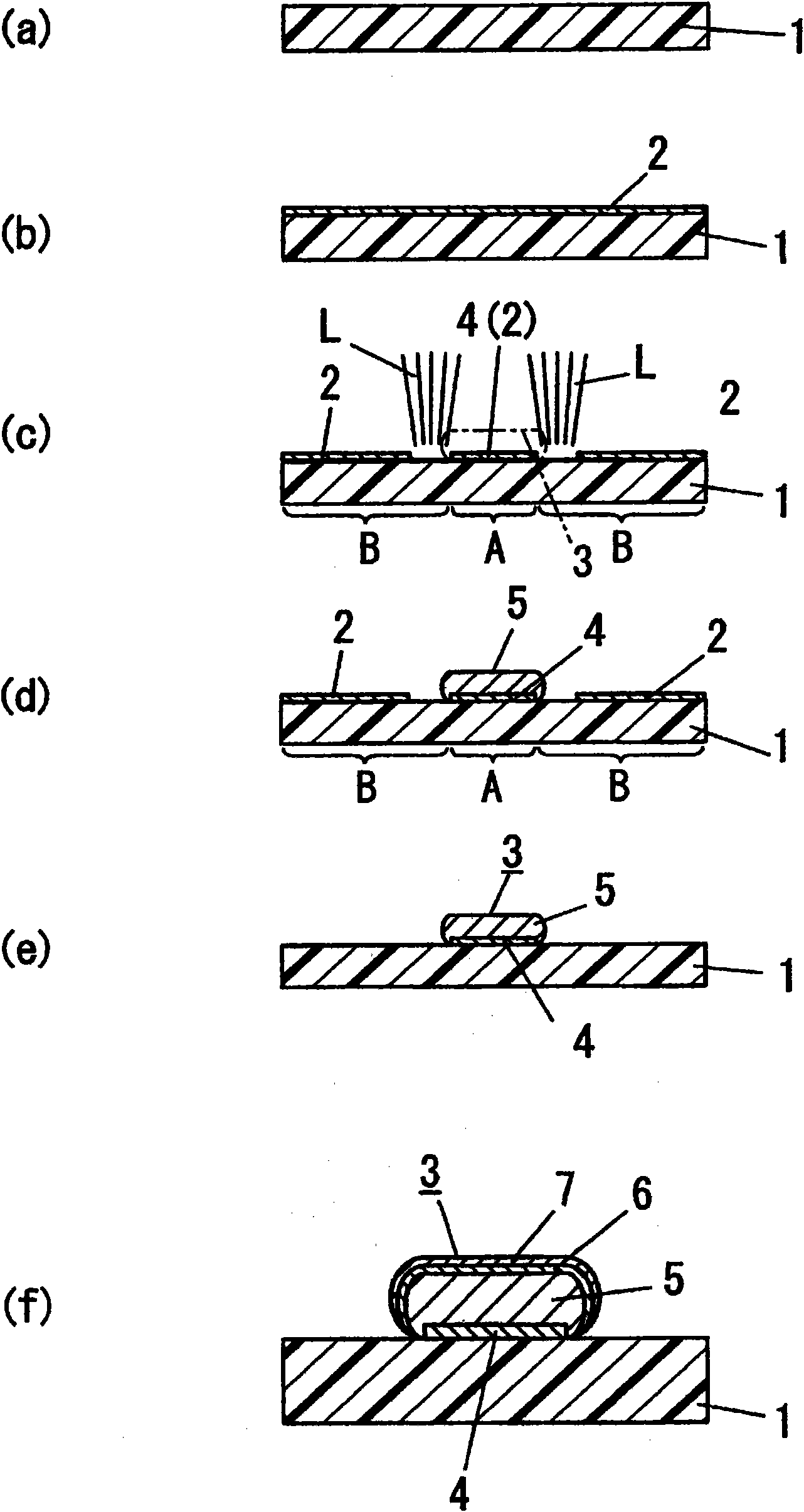
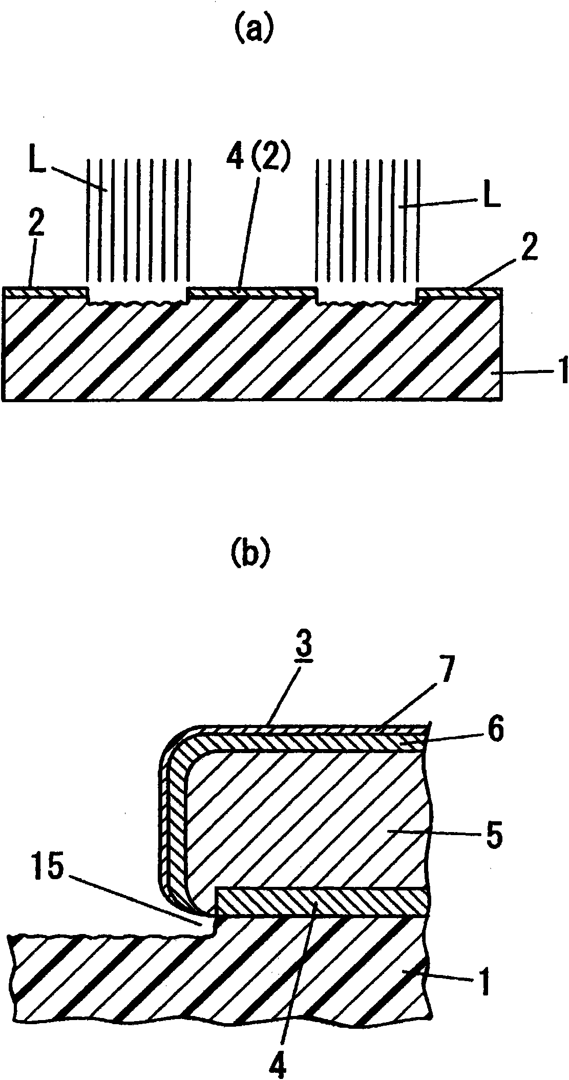
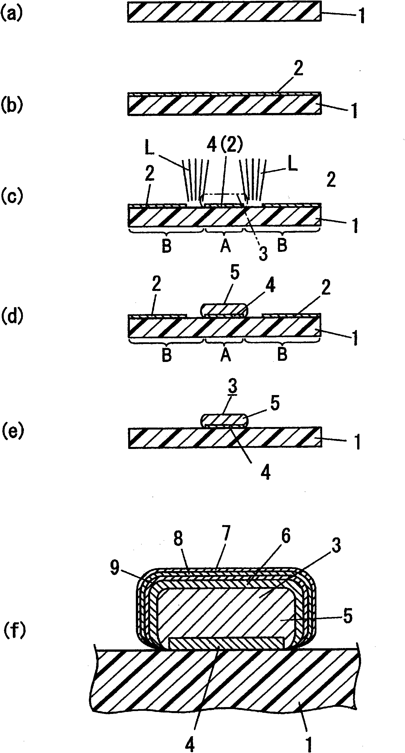
[0066] The insulating substrate 1 was molded using "BT1500" manufactured by Kurashiki Polyester Co., Ltd., a molding material (Kurabo Polyester Co., Ltd.) whose base resin was colored black polyphthalamide ( image 3 (a)). Then, after performing plasma treatment on the surface of the insulating substrate 1, copper was sputtered on the surface of the insulating substrate 1 to form a metal thin film 2 with a film thickness of 0.3 μm ( image 3 (b)).

[0067] Next, the metal thin film 2 is irradiated with a THG-YAG laser L with a wavelength of 355 nm and an output of 0.35 W along the outline of the circuit pattern to carry out laser patterning, thereby forming a plating base layer 4 ( image 3 (c)).

[0068] Next, carry out the copper plating treatment of energization to the base plating layer 4 that is formed by laser drawing, thereby form the copper plating layer 5 on the base plating layer 4 ( image 3 (d)). The copper plating treatment uses a copper sulfate bath composed ...

Embodiment 2

[0076] A circuit board was obtained in the same manner as in Example 1 except that the second intermediate plating layer 9 was formed by palladium plating and the first intermediate plating layer 8 was formed by rhodium plating.

[0077] Here, a palladium plating bath having a Pd concentration of 6 g / L and a pH of 0.8 was used for the palladium plating treatment of the second intermediate plating layer 9 . At a temperature of 55°C and a current density of 0.75A / dm 2 , under the plating conditions of 25 seconds, and the second intermediate plating layer 9 is formed of Pd with a film thickness of 0.1 μm.

[0078] In addition, the first intermediate plating layer 9 containing Rh was formed under the same conditions as in Example 1.

Embodiment 3

[0080] A circuit board was obtained in the same manner as in Example 1 except that the second intermediate plating layer 9 was formed by silver plating and the first intermediate plating layer 8 was formed by rhodium plating.

[0081] Here, the silver plating treatment of the second intermediate plating layer 9 uses a low cyano group bath composed of a bath with a silver concentration of 50 g / L, a free cyano group concentration of 1 g / L, and a Se concentration of 5 mg / L. / dm 2 , under the plating conditions of 15 seconds, and the second intermediate plating layer 9 was formed of Ag with a film thickness of 0.3 μm.

[0082] In addition, the first intermediate plating layer 8 containing Rh was formed under the same conditions as in Example 1.


PUM

PropertyMeasurementUnit
thicknessaaaaaaaaaa

Abstract

A circuit board is provided with an insulating substrate (1) and a circuit (3) formed on the insulating substrate (1). The circuit is provided with a plated base layer (4) whereupon a pattern is formed by irradiating a metal thin film (2) applied on a surface of the insulating substrate (1) with a laser beam (L) along the profile of the circuit (3) and partially removing the metal thin film (2) from the profile of the circuit (3). The circuit is also provided with a Cu-plated layer (5), an Ni-plated layer (6) and an Au-plated layer (7), which are formed by metal plating, on a surface of the plated base layer (4) in this order from the side of the plated base layer. Between the Ni-plated layer (6) and the Au-plated layer (7), a first intermediate plated layer (8) having a less noble metal than Au with respect to reference electrode potential is formed in contact with the Au-plated layer, and a second intermediate plated layer (9) having a more noble metal than the metal in the first intermediate plated layer with respect to the reference electrode potential is formed in contact with the first intermediate plated layer (8).

Description

technical field [0001] The present invention relates to a circuit board in which a circuit is formed on a surface of a planar or three-dimensional insulating substrate and a method for manufacturing the same. Background technique [0002] As a circuit board formed by providing a circuit on the surface of an insulating substrate, a technique of forming a circuit by a pattern generated by laser light has been proposed (for example, refer to Patent Document 1). [0003] In the manufacturing method of the circuit board according to this technique, first as figure 1 As shown in (a), the molded insulating substrate 1 is produced, and then figure 1 As shown in (b), the metal thin film 2 is formed on the entire surface of the insulating substrate 1 by sputtering or the like. Next as figure 1 As shown in (c), along the outline of the circuit 3 to be provided on the surface of the insulating substrate 1, the laser light L is irradiated at the non-circuit forming part B that is an i...

Claims


Application Information

Patent Timeline
Patent Type & Authority Applications(China)
IPC IPC(8): H05K3/24H05K3/08H05K3/18B23K26/00B23K26/36B23K101/42C25D5/12C25D7/00H05K3/00
CPCH05K3/027H05K2201/09363H05K3/108H05K3/244H05K2203/107H05K2203/0723
Inventor 中原阳一郎池川直人上村恭平内野野良幸
Owner PANASONIC CORP
Why Eureka
Try Eureka