Safety film with dynamic three-dimensional effect
A technology of three-dimensional effect and safety film, which is applied in the field of anti-counterfeiting, can solve the problems of low yield, difficulty in releasing UV glue, and decrease in contrast, and achieve the effect of small film thickness
- Summary
- Abstract
- Description
- Claims
- Application Information
AI Technical Summary
Problems solved by technology
Method used
Image
Examples
Embodiment 1
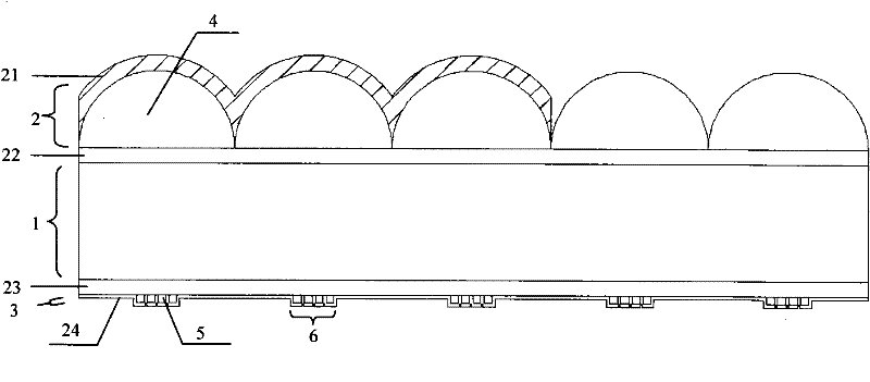
[0061] Embodiment one: see attached figure 1 Shown is a schematic structural diagram of a security film with a dynamic three-dimensional effect. The film has a three-layer structure: substrate layer 1, microlens array layer 2 and micro-nano structured layer 3. There is a micro-nano structure 5 on the micro-graphic layer, and the micro-nano structure 5 forms a micro graphic unit 6 .
[0062] The thickness of the substrate layer 1 is between 10 microns and 5 mm, and preferably the thickness of the substrate layer is between 25 microns and 100 microns. The material of the substrate layer can be PC, PVC, PET, PMMA, UV-sensitive glue or BOPP, etc., preferably, PET.
[0063] The microlens 4 is used to focus light on the micrographic layer 3, and its shape can be hemispherical or ellipsoidal, and its aperture size is 10 to 500 microns, and the preferred microlens 4 aperture size is 25 to 100 microns. The numerical aperture of the microlens is 0.1-4.0, preferably, the numerical ape...
Embodiment 2
[0066] Embodiment two: see attached figure 2 Shown is a structural schematic diagram of a multi-layer security film with a dynamic three-dimensional effect. Can respectively have microlens array protection layer 21, additional layer 22 and 23 and outside microlens array layer 2, substrate layer 1 / microlens array layer 2, substrate layer 1 / micrographic layer 3 and micrographic layer 3 outside Micro-nano structure protection layer 24 . The additional layers 22, 23 and the protective layers 21, 24 can be dielectric layers, metal layers, or coated with ink, fluorescent, magnetic, phosphorous, selective absorption, or have micro-nano structures.
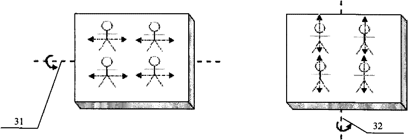
[0067] Accompanying drawing 3 is the schematic diagram showing the effect of a security film with a dynamic three-dimensional effect in Embodiment 1 and Example 2 of the present invention. The security film as described in the first and second examples of the present invention can enlarge the structure originally hidden in the micropat...
Embodiment 3
[0069] Embodiment 3: Refer to Fig. 5 for a schematic example of a regularly arranged microlens array and a microstructure array. The ratio of the area where the microlens is located to the total area is called the duty cycle. The higher the duty cycle, the higher the contrast of the enlarged graphics obtained. Such as Figure 5a The orthogonal array of microlens arrays shown has a duty cycle of 78%, as Figure 5b The shown honeycomb array of microlenses has a duty cycle of up to 90%.
PUM
| Property | Measurement | Unit |
|---|---|---|
| grating period | aaaaa | aaaaa |
| grating period | aaaaa | aaaaa |
| thickness | aaaaa | aaaaa |
Abstract
Description
Claims
Application Information


