
Circuit board

A circuit board and conductive layer technology, applied in the direction of circuit substrate materials, printed circuit components, etc., can solve the problem of different dielectric constants of signal lines, achieve the effect of stabilizing the dielectric constant and reducing the interweaving area

Inactive Publication Date: 2010-10-13
INVENTEC CORP
View PDF0 Cites 1 Cited by
  • Summary
  • Abstract
  • Description
  • Claims
  • Application Information

AI Technical Summary

Problems solved by technology

[0005] The invention provides a circuit board to solve the problem caused by the different dielectric constants of the existing signal lines across the interweaving area

Method used


Image

  • Circuit board
  • Circuit board
  • Circuit board

Examples


Embodiment Construction

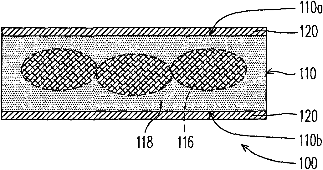
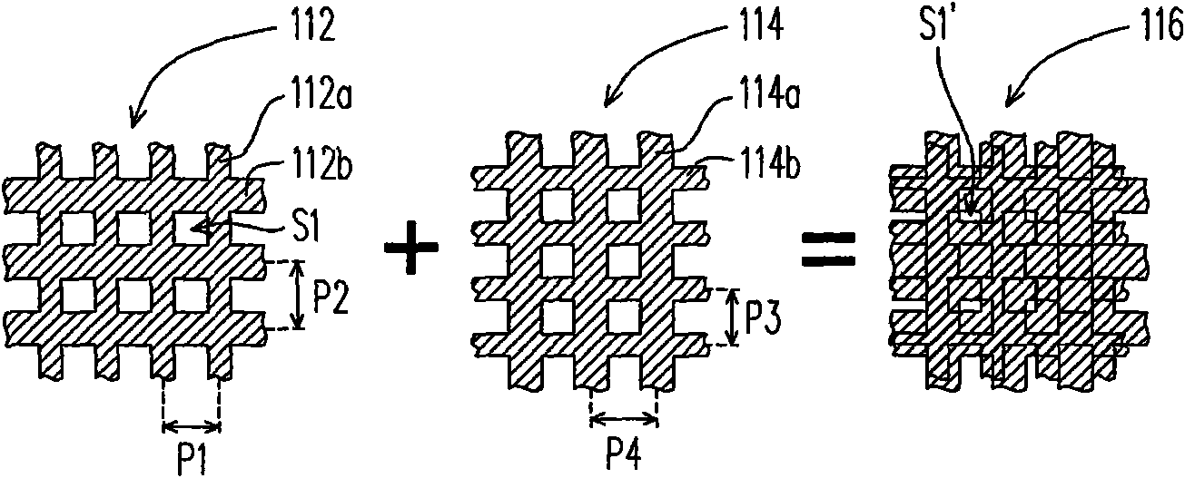
[0028] Figure 1A It is a schematic cross-sectional view of a circuit board according to an embodiment of the present invention, and 1B is Figure 1A Schematic diagrams before and after the superposition of the first glass fiber structure and the second glass fiber structure of the circuit board. Please also refer to Figure 1A and Figure 1B , in this embodiment, the circuit board 100 includes at least one insulating layer 110 ( Figure 1A Only one layer is schematically shown in ) and at least one conductive layer 120 ( Figure 1A Only two layers are schematically shown in the figure), wherein the insulating layer 110 includes at least one first glass fiber structure 112 , at least one second glass fiber structure 114 and a resin material 118 , and the conductive layer 120 is disposed on two opposite sides of the insulating layer 110 on surfaces 110a, 110b. In particular, the conductive layer 120 in this embodiment is a copper foil layer.

[0029] In detail, the first glass...


PUM


Abstract

The invention relates to a circuit board which comprises at least one insulating layer and at least one conducting layer, wherein the insulating layer comprises at least one first glass fiber structure, at least one second glass fiber structure and a resin material; the first glass fiber structure is provided with a plurality of first warp threads and a plurality of first weft threads; the second glass fiber structure is superposed on the first glass fiber structure and provided with a plurality of second warp threads and a plurality of second weft threads; the first warp threads and the first weft threads are not completely superposed with the second warp threads and the second weft threads; the resin material is coated on the first glass fiber structure and the second glass fiber structure; and the conducting layer is arranged on at least one surface of the insulating layer.

Description

technical field [0001] The present invention relates to a circuit board, in particular to a circuit board having a plurality of glass fiber structures that overlap each other and whose warp yarns and weft yarns do not completely overlap. Background technique [0002] A printed circuit board (Printed Circuit Board, PCB) is a multi-layer composite board formed by bonding together a single-layer, double-layer or multi-layer patterned conductive layer and an insulating layer. Generally speaking, the patterned conductive layer is made of extremely thin pure copper metal foil in the printed circuit board, and epoxy resin and glass fiber are used to make the insulation to electrically insulate the two patterned conductive layers. Floor. [0003] Since the interwoven area formed by the warp yarns and the weft yarns of the glass fiber in the existing insulating layer is large, when the patterned conductive layer is disposed on the insulating layer, a part of the signal lines in the ...

Claims


Application Information

Patent Timeline
IPC IPC(8): H05K1/03C08L101/00C08L63/00
Inventor 金新国范文纲
Owner INVENTEC CORP
Learn More