LaAlO3/SrTiO3 heterojunction field effect transistor based on La-based gate and manufacturing method

A heterojunction field effect, transistor technology, applied in semiconductor/solid-state device manufacturing, semiconductor devices, electrical components, etc., can solve the problem that device performance and reliability are difficult to meet requirements, device channel charge control is weakened, device channel Problems such as weak charge control force, to achieve the effect of stable dielectric constant, large forbidden band width, and high dielectric constant

Inactive Publication Date: 2016-04-06
XIDIAN UNIV
View PDF3 Cites 4 Cited by
  • Summary
  • Abstract
  • Description
  • Claims
  • Application Information

AI Technical Summary

Problems solved by technology

At present, the modulation of the flat band voltage of the transition metal oxide heterojunction field effect transistor gate dielectric structure is mainly by changing the Al 2 o 3 The thickness of the dielectric layer is realized, but the adjustable range of this method is small, because increasing the thickness of the gate dielectric layer will lead to the weakening of the control force of the gate capacitance on the channel charge of the device, while reducing the thickness of the gate dielectric layer will lead to the gate pole breakdown current reduction
[0005] In summary, the disadvantages of the gate dielectric materials currently used in transition metal oxide heterojunction field effect transistors are: the dielectric constant is small, resulting in weak control of the gate capacitance on the channel charge of the device. In order to ensure the control of the gate capacitance However, reducing the thickness of the gate dielectric will lead to a decrease in the gate breakdown voltage of the device, which has a strong negative impact on the transconductance of the device, and it is difficult to control the key parameters of the gate dielectric structure of the transition metal oxide heterojunction field effect transistor from the manufacturing process changes, resulting in the performance and reliability of the device is difficult to meet the demand

Method used


Image

  • LaAlO3/SrTiO3 heterojunction field effect transistor based on La-based gate and manufacturing method
  • LaAlO3/SrTiO3 heterojunction field effect transistor based on La-based gate and manufacturing method
  • LaAlO3/SrTiO3 heterojunction field effect transistor based on La-based gate and manufacturing method

Examples


Embodiment 1

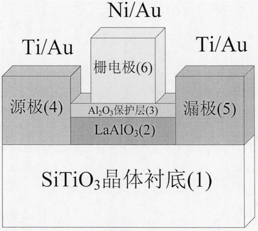
[0036] Embodiment 1: making La 2 o 3 The film thickness is 2nm, Al 2 o 3 LaAlO with stacked gate structure with protective layer thickness of 2nm 3 / SrTiO 3 heterojunction transistors.

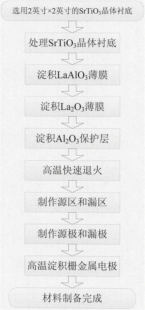
[0037] refer to image 3 , the production steps of this example are as follows:

[0038] Step 1, select SrTiO with a diameter of 1 inch 3 crystal as the substrate, and it is pretreated to obtain the (100) crystal plane, that is, TiO 2 noodle.

[0039] 1a. SrTiO 3 The crystal substrate was placed in deionized water for 20 minutes;

[0040] 1b. Take out SrTiO 3 The crystal substrate, which is placed in a buffer solution consisting of HF at a concentration of 49% and NH at a concentration of 40% 4 Mixture of F, HF and NH 4 The volume ratio of F is 1:5, the pH value is 4.7, soaking for 30 seconds;

[0041] 1c. Take out the SrTiO 3 crystal substrate, the O 2 Under the atmosphere, the temperature was raised to 950°C, and annealing was performed for 1 hour;

[0042] 1d. The annealed ...

Embodiment 2

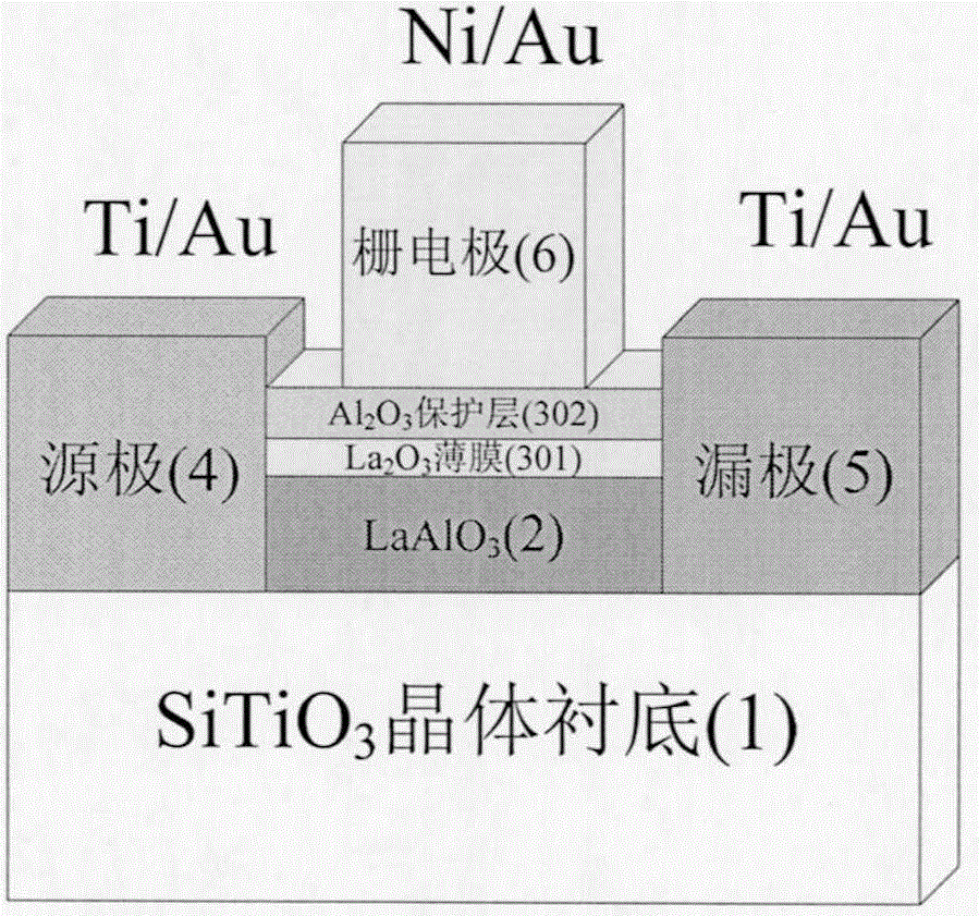
[0082] Embodiment 2: making La 2 o 3 The film thickness is 3nm, Al 2 o 3 LaAlO with stacked gate structure with protective layer thickness of 1nm 3 / SrTiO 3 heterojunction transistors.

[0083] refer to image 3 , the production steps of this example are as follows:

[0084] Step 1, choose SrTiO with a diameter of 1 inch 3 crystal as the substrate, and it is pretreated to obtain the (100) crystal plane, that is, TiO 2 noodle;

[0085] The process of pretreatment is identical with step 2 of example 1.

[0086] Step two, in the pretreated SrTiO 3 Deposit LaAlO with a thickness of 7nm on the crystal substrate 3 film.

[0087] refer to Figure 4 , the specific implementation of this step is as follows:

[0088] 2.1. In the ultra-clean room environment, the pretreated SrTiO 3 Put the crystal substrate into the reaction chamber of the atomic layer deposition equipment, then evacuate the pressure of the chamber to 10hPa, heat the temperature to 320°C, set the nitrogen ...

Embodiment 3

[0119] Embodiment 3: making La 2 o 3 The film thickness is 2nm, Al 2 o 3 LaAlO with stacked gate structure with protective layer thickness of 3nm 3 / SrTiO 3 heterojunction transistors.

[0120] refer to image 3 , the production steps of this example are as follows:

[0121] Step A, select SrTiO with a diameter of 1 inch 3 crystal as the substrate, and it is pretreated to obtain the (100) crystal plane, that is, TiO 2 noodle;

[0122] The process of pretreatment is identical with step 2 of example 1.

[0123] Step B, in the pretreated SrTiO 3 Deposit LaAlO with a thickness of 9 nm on the crystal substrate 3 film.

[0124] refer to Figure 4 , the specific implementation of this step is as follows:

[0125] B1. In the ultra-clean indoor environment, the pretreated SrTiO 3 Put the crystal substrate into the reaction chamber of the atomic layer deposition equipment, then evacuate the pressure of the chamber to 9hPa, heat the temperature to 300°C, set the nitrogen f...


PUM


Abstract

The invention discloses a LaAlO3 / SrTiO3 heterojunction field effect transistor based on a La-based gate and a manufacturing method, and mainly solves the problem in the prior art that gate capacitance has a poor control capability over device channel charges. The LaAlO3 / SrTiO3 heterojunction field effect transistor comprises a SrTiO3 crystal substrate (1) and a LaAlO3 film (2) from bottom to top, and the LaAlO3 film (2) is provided with a source electrode (4), a drain electrode (5) and a gate electrode (6). A gate medium material layer (3) is arranged between the LaAlO3 film (2) and the gate electrode (6) and forms the gate capacitance of the transistor. The gate medium material layer (3) is of a gate stacking structure formed by a La2O3 film (301) and an Al2O3 protection layer (302). According to the invention, the gate medium material is stable in performance and high in dielectric constant, the thermal stability is good, the gate capacitance control capability is high, gate electrode breakdown voltage is high, and the LaAlO3 / SrTiO3 heterojunction field effect transistor based on the La-based gate can be used for manufacturing a high-performance heterojunction field effect transistor device.

Description

technical field [0001] The invention belongs to the technical field of semiconductor materials and devices, in particular to a LaAlO 3 / SrTiO 3 The heterojunction field effect transistor can be used as a transparent display device and a power amplifier device. Background technique [0002] It is well known in the industry that LaAlO with strong correlation properties 3 / SrTiO 3 Transition metal oxide heterointerfaces can be used to fabricate nanoscale field effect transistors, new quantum Hall systems and high-temperature superconductors, and have the potential to be applied to next-generation electronic devices. Due to the strong correlation characteristics of transition metal oxides, the interface will exhibit different properties from the semiconductor interface, and the two-dimensional electron gas formed at the interface is different from the traditional semiconductor interface. In order to apply this property of the transition metal oxide heterojunction interface t...

Claims


Application Information

Patent Timeline
Patent Type & Authority Applications(China)
IPC IPC(8): H01L29/78H01L21/336H01L29/423H01L29/43
CPCH01L29/78H01L29/42364H01L29/432H01L29/66477
Inventor 刘红侠赵璐陈煜海冯兴尧汪星费晨曦
Owner XIDIAN UNIV
Why Eureka
Try Eureka