GaAs enhancing/depletion type strain high mobility of electron transistor material structure

A technology with high electron mobility and material structure, applied in circuits, electrical components, semiconductor devices, etc., can solve problems such as low noise tolerance threshold voltage changes, and achieve the effect of good ohmic contact and high doping rate characteristics

Inactive Publication Date: 2007-02-07
INST OF MICROELECTRONICS CHINESE ACAD OF SCI
View PDF0 Cites 7 Cited by
  • Summary
  • Abstract
  • Description
  • Claims
  • Application Information

AI Technical Summary

Problems solved by technology

However, its disadvantages are low noise tolerance and its sensitivity to changes in threshold voltage. Therefore, a direct coupled FET logic circuit (DCFL) with superior performance must be able to accurately control the threshold voltage of the device
The difficulty in the successful manufacture of integrated enhanceme

Method used


Image

  • GaAs enhancing/depletion type strain high mobility of electron transistor material structure
  • GaAs enhancing/depletion type strain high mobility of electron transistor material structure
  • GaAs enhancing/depletion type strain high mobility of electron transistor material structure

Examples


Embodiment Construction

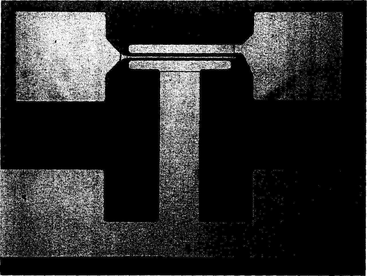
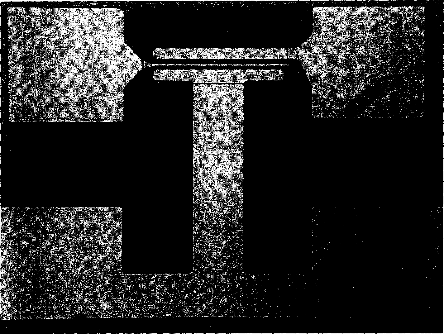
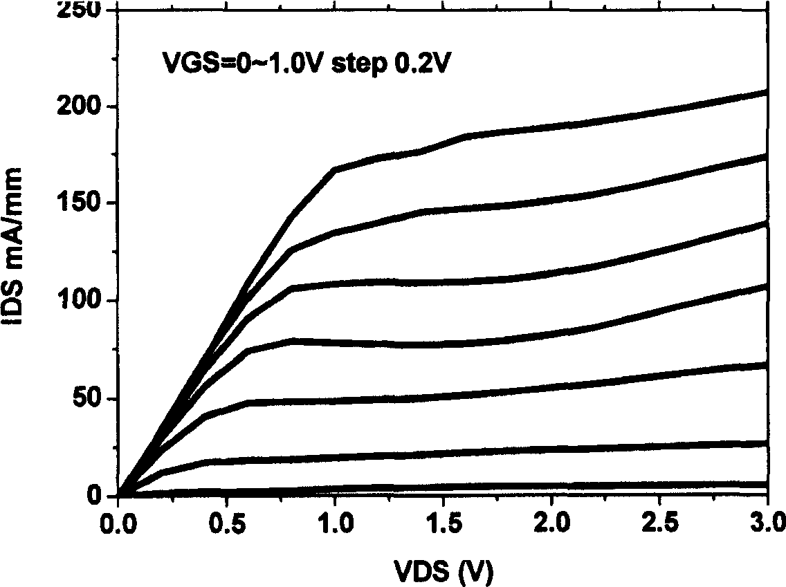
[0025]A gallium arsenide (GaAs) based monolithic integrated enhancement / depletion type strained high electron mobility transistor (MHEMT) device material structure of the present invention, as shown in Table 2, adopts InGaAs / InAlAs / InGaAs Arsenic material structure, on the upper surface of the semi-insulating gallium arsenide (100) substrate material, a linear slow-change InAlGaAs epitaxial layer is grown by slow-change growth technology as a buffer layer with a thickness of 1.5 μm, and then on the buffer layer Sequential growth: the third layer: undoped indium aluminum arsenic layer with a thickness of 500 angstroms; the fourth layer: undoped indium gallium arsenic layer with a thickness of 200 angstroms, indium composition X = 0.53±0.02, gallium group Point Y=0.47±0.02, X+Y=1, as a channel layer; the fifth layer: an undoped indium aluminum arsenic layer, with a thickness of 40 angstroms, as an isolation layer; the sixth layer: a planar doped layer, its The doping concentrati...


PUM


Abstract

The invention relates to an arsenic gallium enhancement/depletion strain high electron mobility transistor structure, wherein it uses indium gallium arsenic/indium aluminum arsenic/indium gallium arsenic material; on the semi-insulated arsenic gallium substrate, it uses slow-change growing technique to grow linear slow-change indium aluminum gallium arsenic extending layer as the buffer layer; then growing indium aluminum arsenic layer, indium gallium arsenic layer, indium aluminum arsenic layer, plane doping layer, indium aluminum arsenic layer, indium phosphor layer, indium aluminum arsenic layer, and indium gallium arsenic layer; the groove two-dimension electron density is 1.57E+12cm-2, the electron mobility is 9790cm2/V.S, with better repeat property and high reliability.

Description

technical field [0001] The invention belongs to the technical field of compound semiconductors, in particular to a gallium arsenide (GaAs)-based monolithic integrated enhancement / depletion strain high electron mobility transistor (MHEMT) material structure. Background technique [0002] High Electron Mobility Transistor (HEMT) devices have by far the highest unity current gain cutoff frequency and lowest noise figure. However, so far, only depletion-mode high electron mobility transistor (HEMT) devices have been widely used in circuit design using high electron mobility transistor (HEMT) devices, such as traditional buffered field effect transistor logic circuits (BFL ) or Source-Coupled Field Effect Transistor Logic (SCFL) are used in actual circuit design, due to the use of depletion-type high electron mobility transistor (HEMT) devices in these circuits, the consequences and shortcomings are the circuit structure Complex and power-hungry. [0003] In order to overcome t...

Claims


Application Information

Patent Timeline
IPC IPC(8): H01L29/201H01L29/78
Inventor 李海鸥尹军舰张海英叶甜春
Owner INST OF MICROELECTRONICS CHINESE ACAD OF SCI
Why Eureka
Try Eureka