High-voltage-resisting GaN-based JBS diode based on gradient drift region and production method of high-voltage-resisting GaN-based JBS diode

A diode, high-voltage technology, used in semiconductor/solid-state device manufacturing, electrical components, circuits, etc., can solve the problems of high breakdown voltage, small turn-on voltage, short reverse recovery time, etc., and reduce quantum tunneling. effect, improved breakdown voltage, high repeatability

Active Publication Date: 2018-06-29
XIDIAN UNIV
View PDF3 Cites 7 Cited by
  • Summary
  • Abstract
  • Description
  • Claims
  • Application Information

AI Technical Summary

Problems solved by technology

The SBD Schottky diode has only one kind of carrier involved in conduction, the reverse recovery time is short, its on-resistance is small, the turn-on voltage is small, but the leakage current is large, and the breakdown voltage is small
[0006] The GaN-based JBS diode combines the advantages of these two diodes, and the cross-sectional structure is as follows: image 3 As shown, although the diode has faster reverse recovery speed and smaller reverse leakage while being able to withstand higher reverse voltage, it cannot fully exert its advantages and cannot reach the expected high breakdown voltage.

Method used


Image

  • High-voltage-resisting GaN-based JBS diode based on gradient drift region and production method of high-voltage-resisting GaN-based JBS diode
  • High-voltage-resisting GaN-based JBS diode based on gradient drift region and production method of high-voltage-resisting GaN-based JBS diode
  • High-voltage-resisting GaN-based JBS diode based on gradient drift region and production method of high-voltage-resisting GaN-based JBS diode

Examples


Embodiment 1

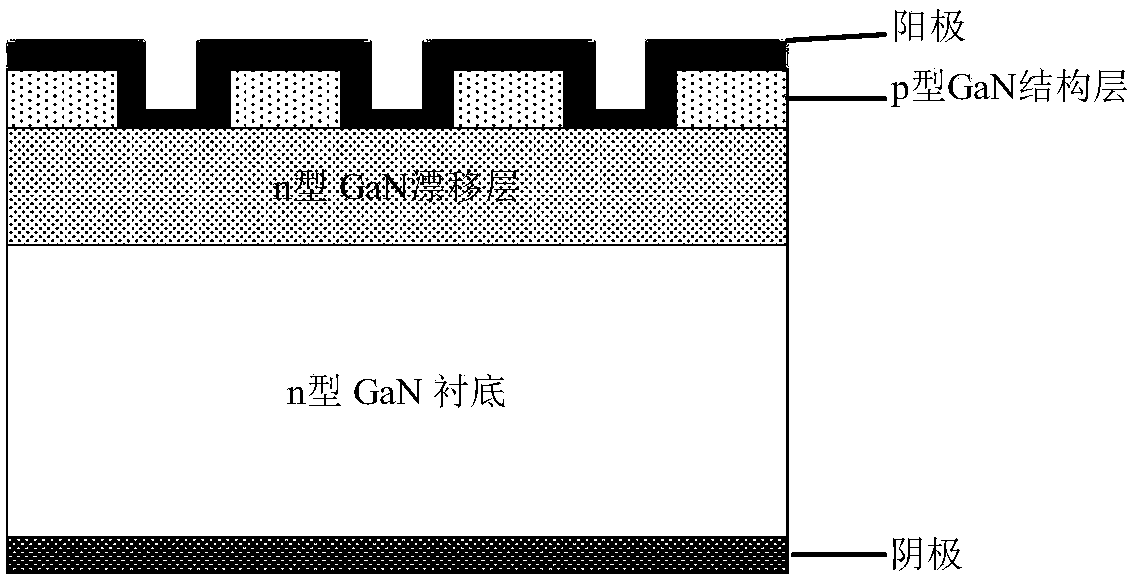
[0046] Example 1, making p-type graded Al composition Al y GaN structure layer and n-type graded Al composition Al x The GaN structure layer is a GaN-based JBS diode with a thickness of 0.1 μm.

[0047] Step 1: Doping the GaN substrate material, such as Figure 5 (a).

[0048] Doping the GaN substrate material with a thickness of 200 μm with Si element, setting SiH 4 The flow rate is 5000sccm, resulting in a doping concentration of 1 × 10 18 cm -3 of n-type GaN substrates.

[0049] Step 2: Grow a GaN drift layer such as Figure 5 (b).

[0050] The GaN drift layer is epitaxially grown on the surface of the n-type GaN substrate using MOCVD equipment, and the doping source is SiH 4 , set SiH 4 The flow rate is 50sccm, the time is 210min, the thickness is 3μm, and the doping concentration is 2×10 16 cm -3 Si-doped n-type GaN drift layer.

[0051] Step 3: Growing n-type Al x GaN structured layers such as Figure 5 (c).

[0052] Epitaxial growth of Al on n-type GaN dr...

Embodiment 2

[0063] Example 2, making p-type graded Al composition Al y GaN structure layer and n-type graded Al composition Al x The GaN structure layer is a GaN-based JBS diode with a thickness of 0.3 μm.

[0064] Step 1: Doping the GaN substrate material with a thickness of 300 μm with Si element to obtain a doping concentration of 1×10 18 cm -3 the n-type GaN substrate, the doping flow is the same as in step 1 of Example 1, such as Figure 5 (a).

[0065] Step 2: Grow a GaN drift layer, such as Figure 5 (b).

[0066] The GaN drift layer is epitaxially grown on the surface of the n-type GaN substrate using MOCVD equipment, and the doping source is SiH 4 , set SiH 4 The flow rate is 150sccm, the time is 420min, the thickness is 6μm, and the doping concentration is 6×10 16 cm -3 Si-doped n-type GaN drift layer.

[0067] Step 3: Growth of n-type Al x GaN structured layers such as Figure 5 (c).

[0068] Epitaxial growth of Al on n-type GaN drift layer using MOCVD equipment x...

Embodiment 3

[0079] Example 3, making p-type graded Al composition Al y GaN structure layer and n-type graded Al composition Al x The GaN structure layer is a GaN-based JBS diode with a thickness of 0.5 μm.

[0080] Step A: Doping the GaN substrate material with a thickness of 400 μm with Si element, setting SiH 4 The flow rate is 5000sccm, resulting in a doping concentration of 1 × 10 18 cm -3 n-type GaN substrates such as Figure 5 (a).

[0081] Step B: Setup SiH 4 The flow rate is 250sccm, the time is 560min, the epitaxial growth thickness is 8μm on the surface of the n-type GaN substrate using MOCVD equipment, and the doping concentration is 10×10 16 cm -3 Si-doped n-type GaN drift layer such as Figure 5 (b).

[0082] Step C: Setup SiH 4 The flow rate is 5000sccm, the time is 35min, and the MOCVD equipment is used to epitaxially grow Al on the n-type GaN drift layer. x GaN structure layer with a thickness of 0.5 μm and a doping concentration of 2×10 18 cm -3 , Si-doped n-...


PUM


Abstract

The invention discloses a high-voltage-resisting GaN-based JBS diode based on a gradient drift region and a production method of the high-voltage-resisting GaN-based JBS diode, and solves the problemthat expected breakdown voltage cannot be reached in the prior art. The high-voltage-resisting GaN-based JBS diode comprises a cathode (1), an n type GaN substrate (2), an n type GaN drift layer (3),an n type AlxGaN structural layer (4), a p type AlyGaN structural layer (5), a plurality of p type GaN structural layers (6) and an anode (7), wherein Al component x of the AlxGaN structural layer isgradually changed from 0 to 0.1, and the doping concentration is 2 to 10x1016cm<-3>; Al component y of the p type AlyGaN structural layer is gradually changed from 0.1 to 0, and the doping concentration is 2x1016cm<-3> to 2x1018cm<-3>. The high-voltage-resisting GaN-based JBS diode disclosed by the invention has the advantages that a quantum tunneling effect is reduced and the breakdown voltage ofa device is improved; in addition, process repeatability and controllability for producing the device are high; the high-voltage-resisting GaN-based JBS diode can be used for a power device.

Description

technical field [0001] The invention belongs to the technical field of semiconductors, and relates to a GaN-based diode device structure and a manufacturing method, which can be used in power devices. Background technique [0002] Power electronics are widely used in various applications and play a key role in power rectification and power switching. GaN-based power devices have attracted wide attention due to their fast switching speed, high operating temperature, high breakdown voltage, and low on-state resistance. The special material properties of GaN itself, such as large band gap, high breakdown field strength, high saturation velocity, and high electron gas density create the superior performance of GaN-based power devices. Today, despite the breakthroughs in GaN-based high electron mobility transistors, there is still a need in the art for improved electronic systems and methods of operating the same. [0003] Compared with planar GaN-based power devices, vertical ...

Claims


Application Information

Patent Timeline
Patent Type & Authority Applications(China)
IPC IPC(8): H01L29/872H01L21/329H01L29/20
CPCH01L29/2003H01L29/66143H01L29/872
Inventor 张进成宋豫秦郝跃党魁张涛边照科
Owner XIDIAN UNIV
Why Eureka
Try Eureka