LED epitaxial growth method used for improving internal quantum efficiency

A technology of internal quantum efficiency and epitaxial growth, which is applied in the field of LED epitaxial growth to improve internal quantum efficiency, can solve the problems of low internal quantum efficiency of electronic leakage current LED, etc., to improve internal quantum efficiency and optical power, improve effective barrier height, Effect of suppressing electron leakage current

Active Publication Date: 2017-12-22
XIANGNENG HUALEI OPTOELECTRONICS
View PDF7 Cites 7 Cited by
  • Summary
  • Abstract
  • Description
  • Claims
  • Application Information

AI Technical Summary

Problems solved by technology

[0006] In view of this, the technical problem to be solved in this application is to provide a LED epitaxial growth method that improves the internal quantum efficiency, and solve the problems of electron leakage current and low internal quantum efficiency of the LED in the existing LED epitaxial growth.

Method used


Image

  • LED epitaxial growth method used for improving internal quantum efficiency
  • LED epitaxial growth method used for improving internal quantum efficiency
  • LED epitaxial growth method used for improving internal quantum efficiency

Examples


Embodiment 1

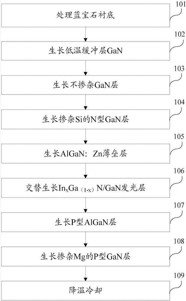
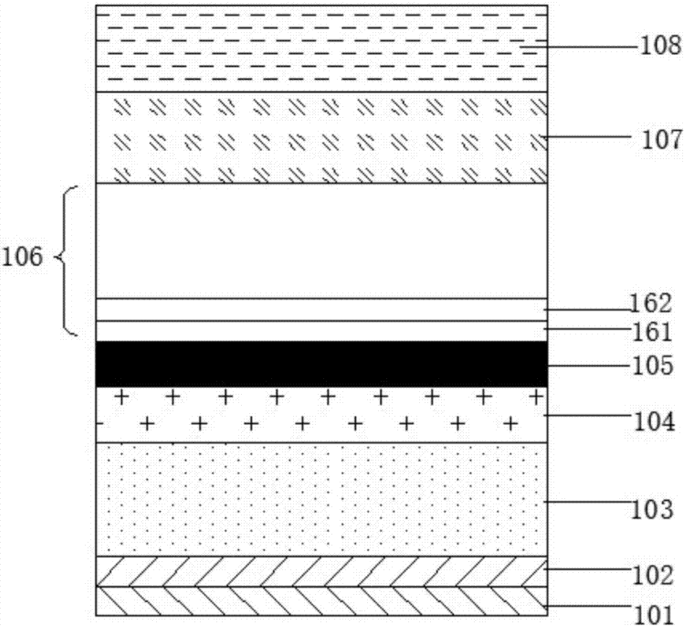
[0051] Such as figure 1 and figure 2 As shown, the LED epitaxial growth method for improving internal quantum efficiency described in this embodiment includes the following steps:

[0052] Step 101, using metal chemical vapor deposition method MOCVD, in 1000°C-1100°C H 2 Under the atmosphere, feed 100L / min-130L / min of H 2 , keep the reaction chamber pressure at 100mbar-300mbar, and process the sapphire substrate for 5min-10min.

[0053] Step 102 , growing a low-temperature buffer layer GaN, and etching the low-temperature buffer layer GaN to form an irregular island shape.

[0054] Step 103 , growing an undoped GaN layer.

[0055] Step 104 , growing a Si-doped N-type GaN layer.

[0056] Step 105, keep the reaction chamber pressure at 800mbar-950mbar, keep the temperature at 750°C-900°C, and feed NH with a flow rate of 50000sccm-55000sccm (sccm is milliliters per minute) 3 , 50sccm-70sccm TMGa, 90L / min-110L / min H 2 , 1200sccm-1400sccm TMAl and 1000sccm-1500sccmDMZn, gro...

Embodiment 2

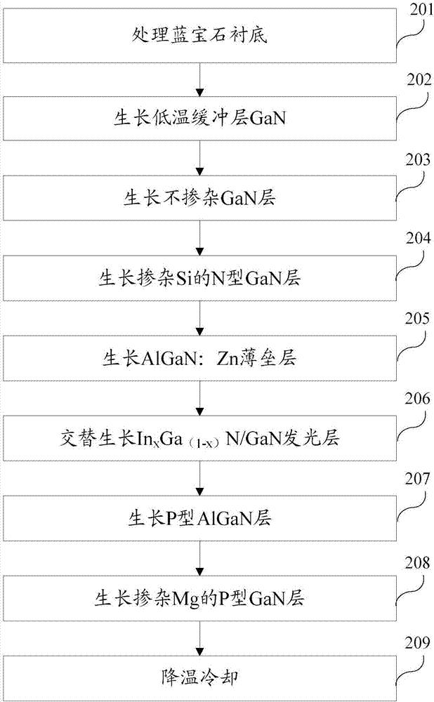
[0065] This embodiment specifically describes the specific content of growing the LED epitaxial layer as a whole, such as image 3 and Figure 4 As shown, the LED epitaxial growth method for improving internal quantum efficiency described in this embodiment includes the following steps:

[0066] Step 201, processing the sapphire substrate: into the reaction chamber of the metal-organic chemical vapor deposition system with the substrate placed, H at 1000°C-1100°C 2 Under the atmosphere, feed 100L / min-130L / min of H 2 , keep the reaction chamber pressure at 100mbar-300mbar, and process the sapphire substrate for 5min-10min.

[0067] Step 202, growing low-temperature buffer layer GaN: lower the temperature to 500°C-600°C, keep the reaction chamber pressure at 300mbar-600mbar, and feed NH with a flow rate of 10000sccm-20000sccm 3 , 50sccm-100sccm TMGa and 100L / min-130L / min H 2 , grow a low-temperature buffer layer GaN with a thickness of 20nm-40nm on a sapphire substrate.

[...

Embodiment 3

[0081] A conventional LED epitaxial growth method is provided below as a comparative example of the present invention.

[0082] Such as Figure 5 and Figure 6 As shown, the conventional LED epitaxial growth method includes the following steps:

[0083] Step 301, processing the sapphire substrate: Into the reaction chamber of the metal-organic chemical vapor deposition system with the substrate placed, H at 1000°C-1100°C 2 Under the atmosphere, feed 100L / min-130L / min of H 2 , keep the reaction chamber pressure at 100mbar-300mbar, and process the sapphire substrate for 5min-10min.

[0084] Step 302, grow low-temperature buffer layer GaN: lower the temperature to 500°C-600°C, keep the reaction chamber pressure at 300mbar-600mbar, and feed NH with a flow rate of 10000sccm-20000sccm 3 , 50sccm-100sccm TMGa and 100L / min-130L / min H 2 , grow a low-temperature buffer layer GaN with a thickness of 20nm-40nm on a sapphire substrate.

[0085] Raise the temperature to 1000°C-1100°C,...


PUM


Abstract

The invention discloses an LED epitaxial growth method used for improving the internal quantum efficiency. The method sequentially comprises the steps of substrate processing, low-temperature buffer layer GaN growing, undoped GaN layer growing, Si-doped N-type GaN layer growing, AlGaN:Zn thin barrier layer growing, alternate InxGa(1-X)N/GaN light emitting layer growing, P-type AlGaN layer growing, Mg-doped P-type GaN layer growing, and cooling. The AlGaN:Zn thin barrier layer grows on one side, which is close to an N-type layer, of a light emitting layer to form an asymmetric well barrier structure to suppress the generation of electron leakage current. The injection efficiency of electrons and holes in a quantum well is improved. The internal quantum efficiency and the optical power of an LED are improved. The light emitting efficiency of the LED is enhanced.

Description

technical field [0001] The present application relates to the technical field of LED epitaxial growth, in particular to an LED epitaxial growth method for improving internal quantum efficiency. Background technique [0002] As a lighting source, LED has the advantages of low energy consumption, long life, small size, high luminous efficiency, no pollution and rich colors compared with existing conventional lighting sources. At present, the scale of domestic production of LEDs is gradually expanding, and the market demand for LEDs and LED light effects are increasing day by day. [0003] Since the quantum efficiency of LEDs is still not high at present, the luminous efficiency of LEDs cannot be improved in a breakthrough, which has become the most concerned issue in the industry. [0004] At present, gallium nitride materials are mostly used in quantum wells in LEDs. Gallium nitride materials have a brazingite structure. Due to the self-polarization effect of the material it...

Claims


Application Information

Patent Timeline
Patent Type & Authority Applications(China)
IPC IPC(8): H01L33/00H01L33/04H01L33/14H01L33/32
CPCH01L33/0066H01L33/0075H01L33/04H01L33/14H01L33/32
Inventor 徐平
Owner XIANGNENG HUALEI OPTOELECTRONICS
Why Eureka
Try Eureka