Deep ultraviolet light emitting diode and preparation method thereof
A light-emitting diode, deep ultraviolet technology, applied in semiconductor devices, electrical components, circuits, etc., can solve the problems of insufficient carrier injection, enhanced hole injection, complex process, etc., to improve external quantum efficiency and increase hole concentration , Improve the effect of optical power
- Summary
- Abstract
- Description
- Claims
- Application Information
AI Technical Summary
Problems solved by technology
Method used
Image
Examples
Embodiment 1
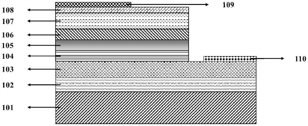
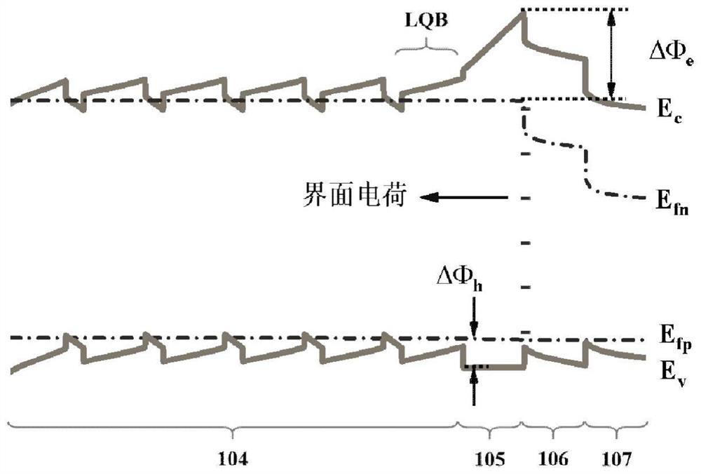
[0047] A deep ultraviolet light-emitting diode in this embodiment, along the epitaxial growth direction, the epitaxial layer structure is a substrate 101, a buffer layer 102, an n-type semiconductor electron injection layer 103, a multi-quantum well active layer 104, and an AlGaN insertion layer 105 , p-type electron blocking layer 106 , p-type semiconductor hole injection layer 107 , p-type contact layer 108 , p-type electrode 109 , and n-type electrode 110 .
[0048] In the above, the material of the substrate 101 is sapphire, and the material of the buffer layer 102 is Al x1 Ga 1-x1 The value of N, x1 is 1, that is, the material of the buffer layer is AlN, the thickness is 100nm, and the material of the n-type semiconductor electron injection layer 103 is n-Al 0.6 Ga 0.4 N, with a doping concentration of 8e18 cm -3 , with a thickness of 4um, the material of the multi-quantum well active layer 104 is alternately grown barrier layers Al 0.57 Ga 0.43 N and well layer Al ...
Embodiment 2
[0065] Other steps in this embodiment are the same as in Embodiment 1, the difference is that the material of the AlGaN insertion layer 105 in this embodiment is Al y Ga 1-y N (y=0.57-0.65), y increases from 0.57 to 0.65 along the direction of epitaxial growth, and the thickness of the insertion layer is 20nm.
Embodiment 3
[0067] Other steps in this embodiment are the same as embodiment 1, and the difference is that the barrier layer is Al in this embodiment 0.6 Ga 0.4 N, the material of the p-type electron blocking layer 106 is p-Al 0.7 Ga 0.3 N, the material of the AlGaN insertion layer is Al y Ga 1-y N (y=0.6-0.85), y increases from 0.6 to 0.85 along the direction of epitaxial growth, and the thickness of the insertion layer is 10 nm.
PUM
| Property | Measurement | Unit |
|---|---|---|
| thickness | aaaaa | aaaaa |
| thickness | aaaaa | aaaaa |
| thickness | aaaaa | aaaaa |
Abstract
Description
Claims
Application Information


