Gallium nitride-based light-emitting diode epitaxial wafer and manufacturing method thereof

A light-emitting diode, gallium nitride-based technology, applied in semiconductor devices, electrical components, circuits, etc., can solve the problems of decreased internal quantum efficiency, unfavorable electron overflow, energy band tilt, etc., so as to improve internal quantum efficiency and improve energy efficiency. Band inclination, the effect of alleviating the bending of the energy band

Active Publication Date: 2020-04-14
HC SEMITEK ZHEJIANG CO LTD
View PDF0 Cites 0 Cited by
  • Summary
  • Abstract
  • Description
  • Claims
  • Application Information

AI Technical Summary

Problems solved by technology

The compressive stress will generate a piezoelectric polarization electric field, which will cause the inclination of the energy band, which is not conducive to blocking the overflow of electrons to the P-type layer. At the same time, it will also affect the injection of holes into the multi-quantum well layer, so that the wave functions of electrons and holes overlap. decrease, resulting in a decrease in the internal quantum efficiency of the LED

Method used


Image

  • Gallium nitride-based light-emitting diode epitaxial wafer and manufacturing method thereof
  • Gallium nitride-based light-emitting diode epitaxial wafer and manufacturing method thereof

Examples


Embodiment Construction

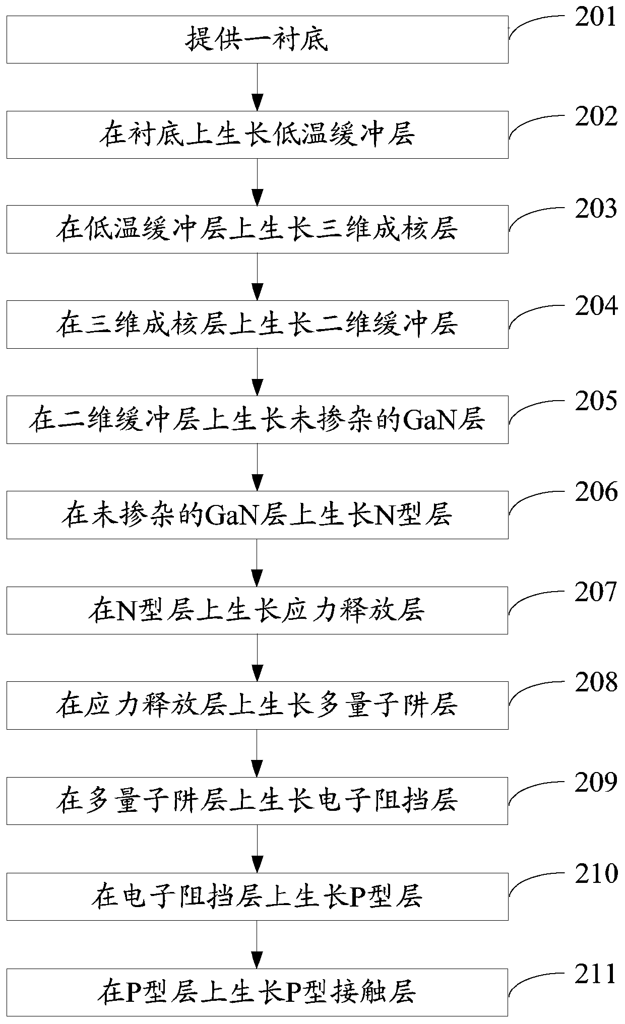
[0030] In order to make the object, technical solution and advantages of the present invention clearer, the implementation manner of the present invention will be further described in detail below in conjunction with the accompanying drawings.

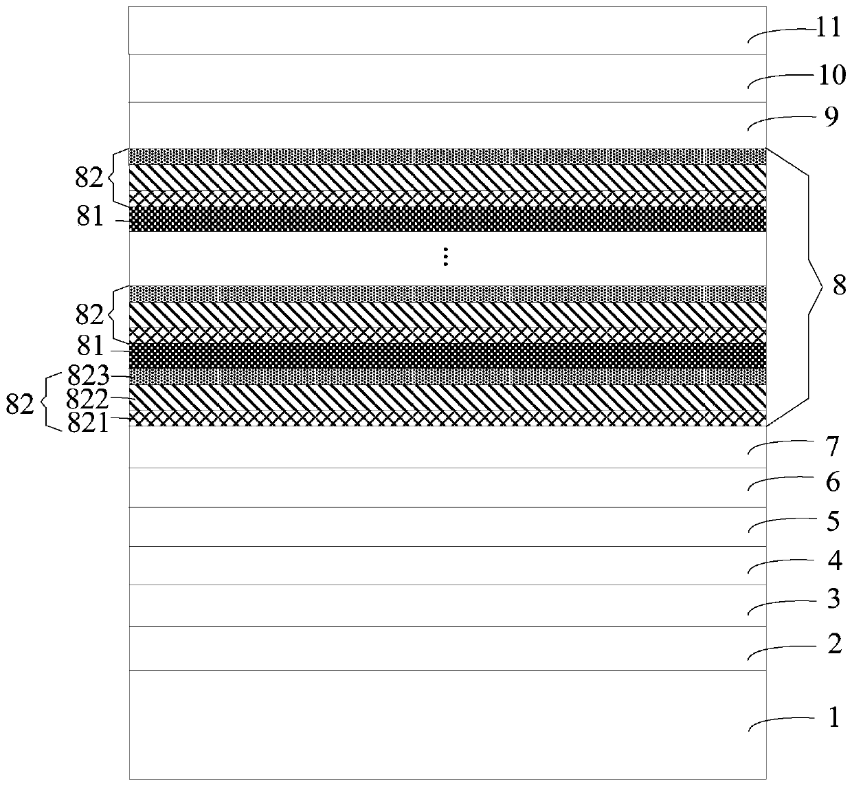
[0031] figure 1 It is a schematic structural diagram of a gallium nitride-based light-emitting diode epitaxial wafer provided by an embodiment of the present invention, as shown in figure 1 As shown, the light-emitting diode epitaxial wafer includes a substrate 1, and a low-temperature buffer layer 2, a three-dimensional nucleation layer 3, a two-dimensional recovery layer 4, an undoped GaN layer 5, and an N-type layer 6 grown on the substrate 1 in sequence. , multi-quantum well layer 8 , electron blocking layer 9 , and P-type layer 10 .

[0032] The multi-quantum well layer 8 includes a plurality of quantum well layers 81 and a plurality of quantum barrier layers 82 grown alternately, and each quantum barrier layer 82 includes a firs...


PUM

PropertyMeasurementUnit
thicknessaaaaaaaaaa
thicknessaaaaaaaaaa
thicknessaaaaaaaaaa

Abstract

The invention discloses a gallium nitride-based light emitting diode epitaxial wafer and a production method thereof and belongs to the technical field of a semiconductor. The gallium nitride-based light emitting diode epitaxial wafer comprises a substrate, and a low temperature buffer layer, a three-dimensional nucleating layer, two-dimensional recovery layer, an undoped GaN layer, an N-type layer, multiple quantum well layers, an electron barrier layer and a P-type layer which are grown on the substrate in sequence. Multiple quantum well layers comprise a plurality of quantum well layers anda plurality of quantum barrier layers which are grown alternately. Each quantum barrier layer comprises a first sub-layer, a second sub-layer and a third sub-layer which are laminated in sequence. The first sub-layers, the second sub-layers and the third sub-layers are BGaN layers. Mg is doped in the second sub-layers. According to the gallium nitride-based light emitting diode epitaxial wafer provided by the invention, electron overflow and hole injection can be improved, so internal quantum efficiency of an LED is improved.

Description

technical field [0001] The invention relates to the technical field of semiconductors, in particular to a gallium nitride-based light-emitting diode epitaxial wafer and a manufacturing method thereof. Background technique [0002] LED (Light Emitting Diode, Light Emitting Diode) is a semiconductor electronic component that can emit light. As an efficient, environmentally friendly and green new solid-state lighting source, it is being rapidly and widely used, such as traffic lights, car interior and exterior lights, urban landscape lighting, mobile phone backlights, etc. [0003] The epitaxial wafer is the main component of the LED. The existing GaN-based LED epitaxial wafer includes a substrate, a low-temperature buffer layer, a three-dimensional nucleation layer, a two-dimensional recovery layer, and an undoped GaN layer stacked on the substrate in sequence. , an N-type layer, a multi-quantum well layer, an electron blocking layer and a P-type layer, wherein the multi-quan...

Claims


Application Information

Patent Timeline
Patent Type & Authority Patents(China)
IPC IPC(8): H01L33/06H01L33/14H01L33/32H01L33/00
Inventor 陶章峰程金连张武斌乔楠李鹏胡加辉
Owner HC SEMITEK ZHEJIANG CO LTD
Why Eureka
Try Eureka