Method for bonding copper wire of power device

A power device and copper wire technology, which is applied in the field of semiconductor discrete device packaging technology, can solve problems such as the decrease of the bonding force between the copper wire ball and the chip, the increase of the surface hardness of the copper wire ball, and the damage of the semiconductor chip, so as to increase product reliability, Simple implementation, the effect of reducing the saturation pressure drop parameter value

Inactive Publication Date: 2010-10-20
深圳市贵鸿达电子有限公司
View PDF7 Cites 20 Cited by
  • Summary
  • Abstract
  • Description
  • Claims
  • Application Information

AI Technical Summary

Problems solved by technology

Compared with gold wire, copper wire is characterized by strong electrical conductivity, low price, high hardness, and good mechanical properties, but it is extremely easy to oxidize. Burning ball oxidation of copper wire will cause the surface hardness of copper wire ball to increase. When bonding Cause damage to the semiconductor chip, and because of the ba

Method used


Image

  • Method for bonding copper wire of power device
  • Method for bonding copper wire of power device
  • Method for bonding copper wire of power device

Examples


Embodiment 1

[0066] According to the parameters corresponding to Embodiment 1 in Table 6, the bonding of the power device is performed, and the steps are as follows:

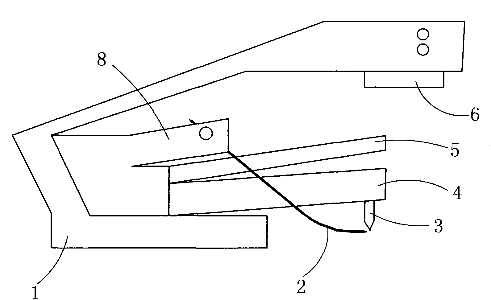
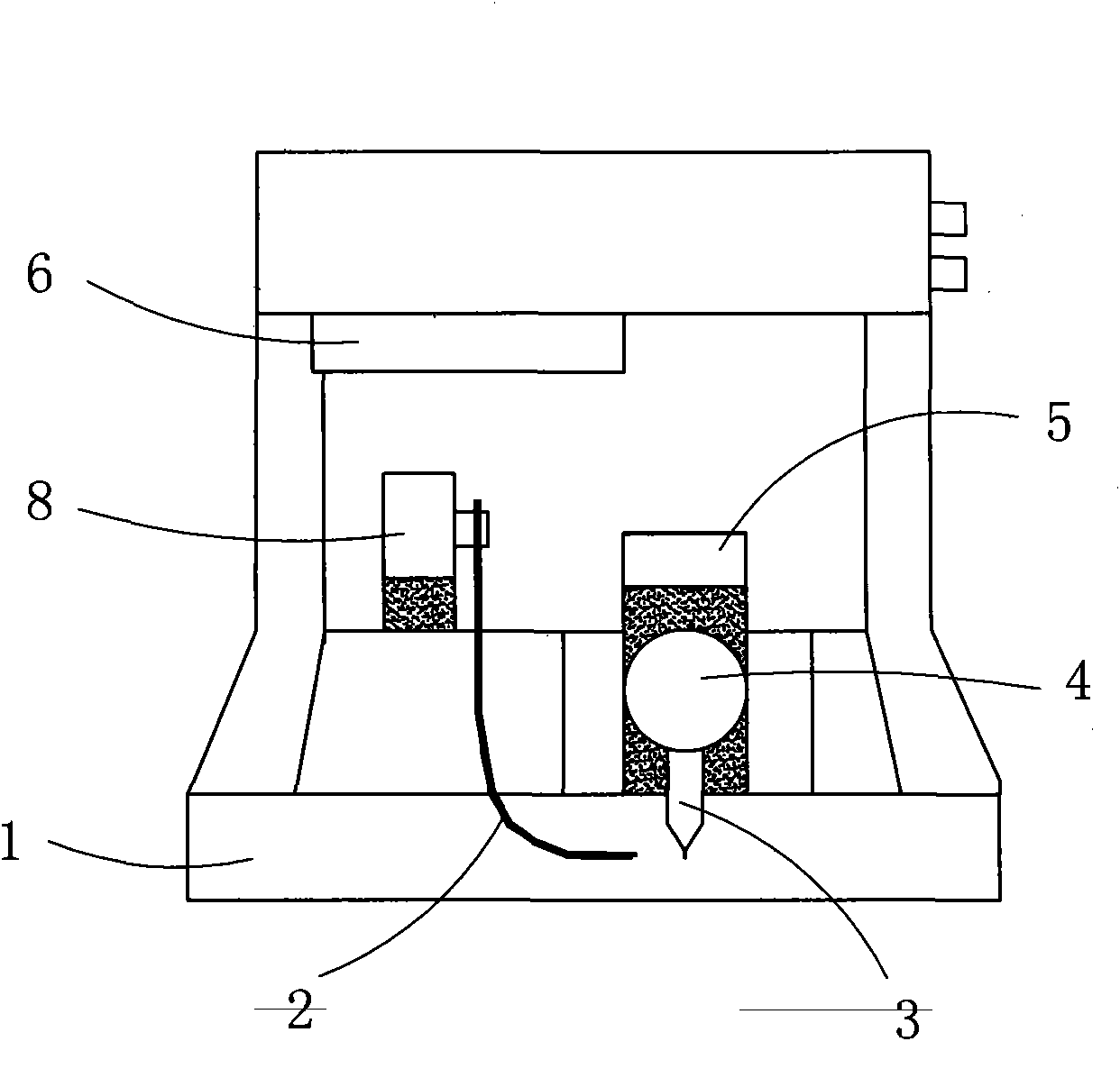
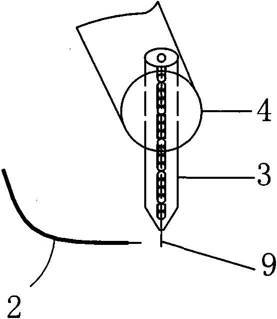
[0067] 1. Open the first blowing pipe 10 and the second blowing pipe 20 to make N 2 and H 2 The mixed gas continuously blows the burning ball position and implements blowing protection (see Figure 4 ), the gas flow rate in the first blowing pipe is 0.3-0.5 liters / minute, and the gas flow rate in the second blowing pipe is 0.5-0.7 liters / minute;

[0068] 2. The wire feeder 5 releases the copper wire through the porcelain mouth 3, and the lower end 9 of the copper wire protrudes and is located at the outer end of the lighter 2;

[0069] 3. The sparker 2 releases high-voltage electricity to burn the lower end 9 of the copper wire into a spherical shape, because there is N 2 and H 2 The protection of the mixed gas, the copper wire ball is not oxidized;

[0070] 4. Use the porcelain nozzle 3 to apply pre-pressure to the sph...

Embodiment 2~9

[0076] According to the test parameters of Examples 2 to 9 in Table 6, the same steps as in Example 1 are used for bonding, and the obtained test results are shown in Table 6 for each of Examples 2 to 9. It can be seen that using 1.5mil It is feasible to bond the copper wire and Huajing 1.48×1.48 chip under the parameters of Examples 2-9.

[0077] The flow rate of the mixed gas can be 0.5 liters / minute, 0.6 liters / minute, 0.7 liters / minute, and it is all feasible in the range of 0.5-0.7 liters / minute.

Embodiment 10~18

[0079] Respectively according to the test parameters of Examples 10-18 in Table 7, the steps of Example 1 are used for bonding, and the obtained test results are shown in the respective correspondences of Examples 10-18 in Table 7. It can be seen that using 1.2mil copper wire and 1.3×1.3 chips from Shenai Company are all feasible for bonding under the parameters of Examples 10-18.


PUM


Abstract

The invention provides a method for bonding a copper wire of a power device, in particular to a method for bonding the copper wire (91) with the welding joints of a chip (511). The method comprises the following steps: burning the lower end (9) of the copper wire into a spherical shape; applying the pre-pressure on the spherical end of the copper wire, i.e., flattening the spherical end of the copper wire to increase the contact area of the spherical end of the copper wire and the chip; and welding the spherical end of the copper wire to the bonding area of the chip on an ultrasonic-welding basis, wherein the pre-pressure is preferably 80g to 120g, and the time for applying the pre-pressure is preferably 80ms to 150ms. By increasing the contact area, the invention can improve the stability and reliability in welding the copper wire and the chip; the bonding production can be smooth without breaking the copper wire, breaking the welding joints or shutting down; the chip cannot be damaged by bonding; and the bonding strength of the copper wire, the chip and the pin is high. By substituting the copper wire for the gold wire for bonding, the invention can reduce the cost for the bonding metal wire by about 84%, reduce the overall cost for the product by 5.7% to 8.6%, reduce the saturation voltage drop parameter of the product and improve the reliability of the product; and compared with the gold wire, the conductivity of the copper wire is increased by about 20%, thus improving the reliability of the product.

Description

technical field [0001] The invention relates to semiconductor discrete device packaging technology, in particular to a bonding process using copper wires instead of gold wires, that is, a process method for connecting the B and E poles of a chip with two pins of a lead frame with copper wires. Background technique [0002] Bonding refers to the process of connecting the B and E poles of the chip with the two pins of the lead frame by ultrasonic welding with gold wires (or copper wires), in order to increase the contact area between the gold wires (or copper wires) and the chip , to improve the bonding strength and electrical conductivity of copper wires, chips, and pins. Before the chip solder joints are bonded, the bonding equipment uses a torch to release high-voltage electricity to burn the ends of the gold wires (or copper wires) into balls, and then pass Ultrasonic welding to the bonding area of ​​the chip, and the pins do not need to burn the ball to ensure the bonding...

Claims


Application Information

Patent Timeline
IPC IPC(8): B23K20/24B23K20/10H01L21/607
CPCH01L2224/48091H01L24/78H01L2224/48247H01L2224/48465H01L2224/78301H01L2924/3025H01L2224/45144H01L2224/85181H01L2924/00014H01L2224/49171H01L2224/05624H01L2224/78H01L2224/85H01L2224/85439H01L2924/00011H01L2924/10253H01L2924/00H01L2224/45147H01L2924/00012H01L2924/01005H01L2924/01004H01L2924/00015H01L2924/01033
Inventor 刘卫光颜文李西萍
Owner 深圳市贵鸿达电子有限公司
Why Eureka
Try Eureka