Method and device for measuring thickness of semiconductor film

A thin film thickness, semiconductor technology, applied in the direction of mechanical thickness measurement, etc., can solve the problem of large amount of data, to achieve the effect of improving efficiency, improving fitting efficiency, and improving accuracy

Active Publication Date: 2010-10-20
ENN SOLAR ENERGY
View PDF3 Cites 22 Cited by
  • Summary
  • Abstract
  • Description
  • Claims
  • Application Information

AI Technical Summary

Problems solved by technology

Analysis according to the existing technology requires 4.2E(10)

Method used


Image

  • Method and device for measuring thickness of semiconductor film
  • Method and device for measuring thickness of semiconductor film
  • Method and device for measuring thickness of semiconductor film

Examples


Embodiment Construction

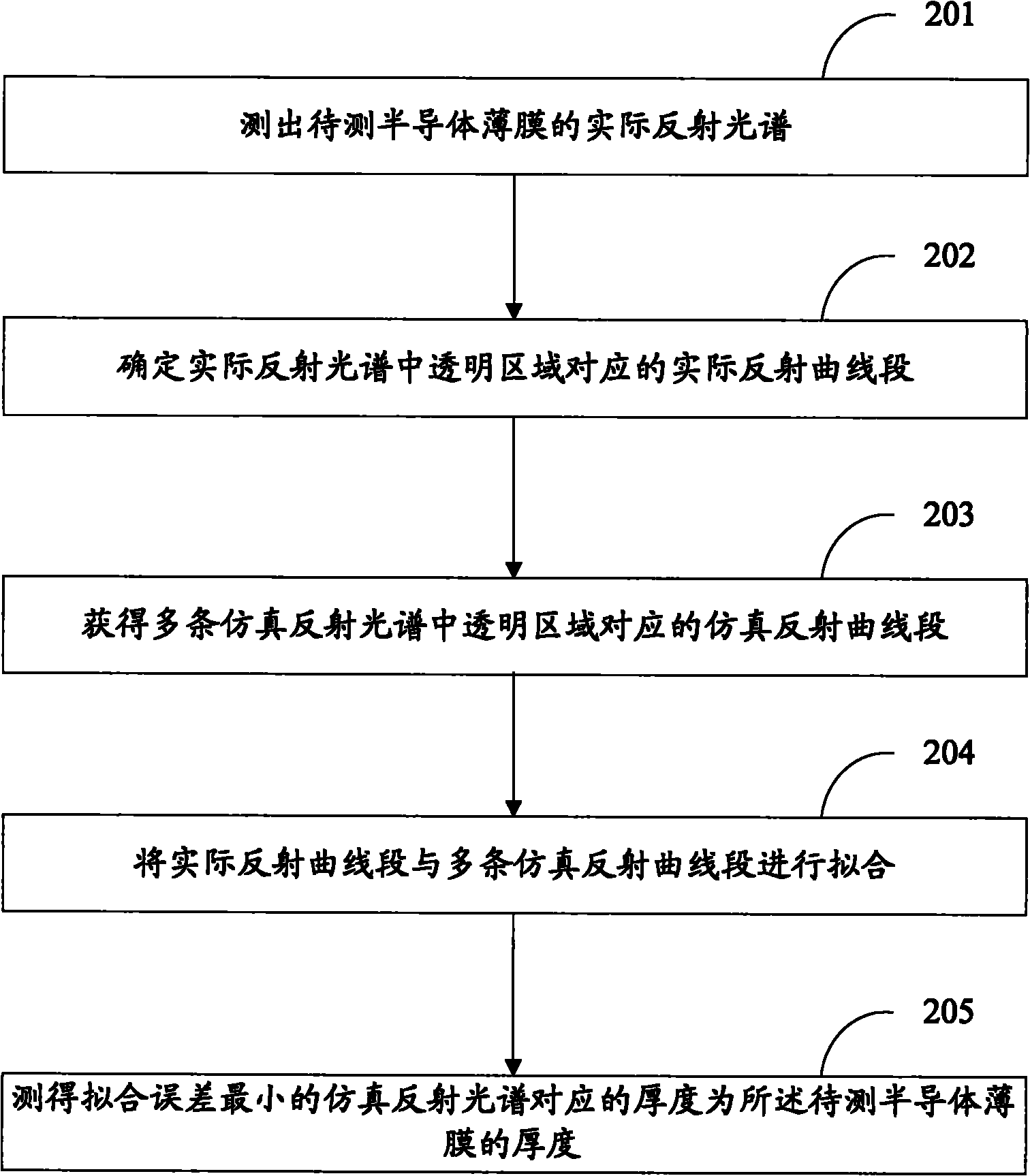
[0041] In the embodiment of the present invention, the transparent area of ​​the actual reflection spectrum is fitted with the transparent areas of multiple simulated reflection spectra, and then the thickness corresponding to the simulated reflection spectrum with the smallest fitting error is measured as the thickness of the semiconductor film to be tested. In this way, in the embodiment of the present invention, the influence of the absorption region of the reflection spectrum on the fitting result is reduced, the accuracy of the fitting result is improved, and a more accurate film thickness is obtained. And because the partial reflection spectrum is used for fitting instead of the complete reflection spectrum, the fitting efficiency is improved, thereby improving the efficiency of obtaining the film thickness.

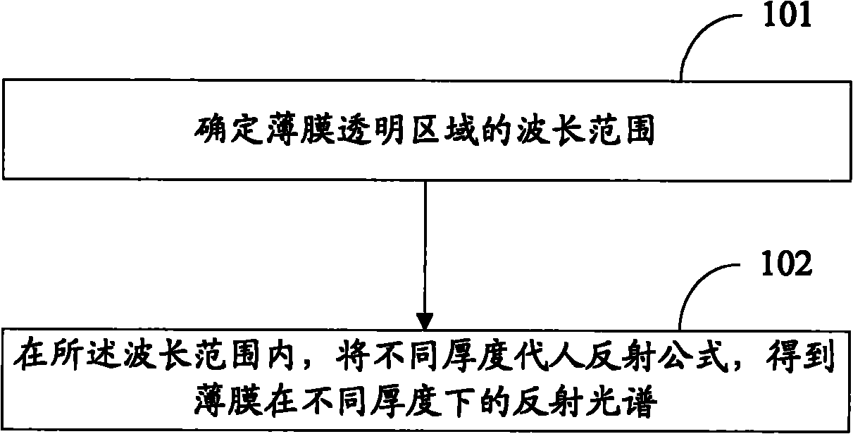
[0042] See figure 1 The process of the method for obtaining the simulated reflection spectrum of the film in this embodiment is as follows:

[0043] Step 101: Determine...


PUM


Abstract

The invention discloses a method for measuring the thickness of a semiconductor film, which is used for improving the efficiency of calculating film thickness and obtaining more accurate film thickness. The method comprises the following steps: measuring an actual reflection spectrum of the semiconductor film to be measured; determining an actual curve section corresponding to a transparent region in the actual reflection spectrum; obtaining simulated reflection curve sections corresponding to transparent regions in a plurality of simulated reflection spectra, wherein the plurality of simulated reflection spectra comprise reflection spectra of different thicknesses of film samples with the same reflective index as the semiconductor film to be measured; fitting the actual reflection curve sections and the plurality of simulated reflection curve sections; and measuring the thickness corresponding to the simulated reflection spectrum with the minimum error of fitting to be used as the thickness of the semiconductor film to be measured. The invention also discloses a device for realizing the method.

Description

Technical field [0001] The present invention relates to the field of semiconductors and optics, in particular to a method and device for measuring the thickness of a semiconductor film. Background technique [0002] Using a spectrophotometer to measure the thickness of semiconductor films is a very important and widely used technique. The basic principle of this technique is to find the matching refractive index, extinction coefficient and membrane thickness. [0003] One of the existing technologies is to manually input the refractive index n and extinction coefficient k of the film, and on this basis, the film thickness is calculated by theoretical fitting. Due to the complexity of the microstructure of the film samples, the refractive index n and extinction coefficient k of different film samples are not exactly the same. Therefore, the optical parameters input manually and the actual optical parameters of the film often have large deviations, which will cause the analysis resu...

Claims


Application Information

Patent Timeline
IPC IPC(8): G01B5/06
Inventor 张晓勇郭铁
Owner ENN SOLAR ENERGY
Why Eureka
Try Eureka