Preparation method of nanometer silicon quantum dots and application thereof in film solar batteries

A technology of nano-silicon quantum dots and thin-film solar cells, which is applied in the manufacture of circuits, electrical components, and final products, and can solve the problems that the efficiency of nano-silicon or microcrystalline silicon thin-film solar cells has not been greatly improved.

Inactive Publication Date: 2010-10-20
CHANGZHOU UNIV
View PDF6 Cites 14 Cited by
  • Summary
  • Abstract
  • Description
  • Claims
  • Application Information

AI Technical Summary

Problems solved by technology

[0004] However, the efficiency of nano-silicon or microcrystalline silicon thin-film solar cells r

Method used


Image

  • Preparation method of nanometer silicon quantum dots and application thereof in film solar batteries
  • Preparation method of nanometer silicon quantum dots and application thereof in film solar batteries
  • Preparation method of nanometer silicon quantum dots and application thereof in film solar batteries

Examples


Embodiment Construction

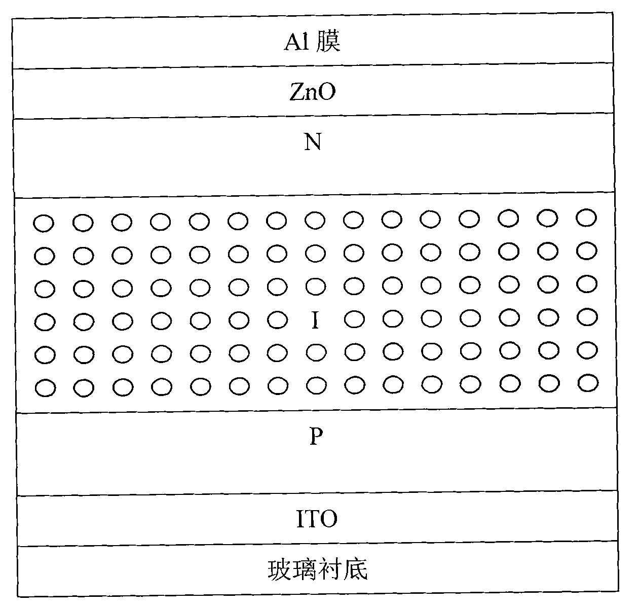
[0024] Preparation of Nano-Silicon Quantum Dots

[0025] 1. Growth of amorphous silicon on glass by PECVD method

[0026] Background vacuum 1.0×10 -4 Pa, the RF frequency is 13.56MHz, the RF power is 120W, and the deposition temperature is 180°C. The dilution ratio of the silane used is 5%, the silane flow rate is 30 sccm, the hydrogen gas flow rate is 30 sccm, and the growth thickness of amorphous silicon is about 500 nm.

[0027] 2. Use double beams to scan layer by layer to crystallize the amorphous silicon film.

[0028] The specific parameters of the femtosecond laser are: the central wavelength of the output of the titanium sapphire regenerative amplifier laser is 800nm, and the 400nm linearly polarized light whose polarization direction is perpendicular to the fundamental frequency of 800nm ​​light can be obtained through frequency doubling of the KDP crystal. The polarization state of the second laser is converted to circular polarization, and the laser energy incid...


PUM


Abstract

The invention aims at providing a preparation method of nanometer silicon quantum dots and application of the method in the manufacture of film solar batteries. The invention uses a PECVD method for growing amorphous silicon, and adopts double light beams for scanning the crystalline amorphous silicon films layer by layer, i.e. the double-light-beam interference of two beams of femtosecond lasers with the polarization state of round polarization state is used for forming nanometer crystalline silicon in amorphous lattices, and the scanning on the amorphous silicon by the double beams of the femtosecond lasers layer by layer utilizes the movement of a three-dimensional sample table. First, the femtosecond laser is gathered at a point in the sample, and the laser carries out plane scanning on the samples in the depth of the sample in a way of moving scanning line by line. After the scanning of the layer is completed, the sample table is moved up, and the laser is gathered on an upper plane again for scanning. Through regulating and controlling the laser power, the pulse width, the repeating frequency and the scanning speed, nanometer silicon arrays with the size distribution of the crystal grains in a range from 30 to 50 nm and the crystal grain space controlled between 20 and 40 nm are formed in the amorphous silicon lattices, the nanometer silicon quantum dot layer can be used for manufacturing silicon base film batteries, and the battery conversation efficiency can be improved.

Description

technical field [0001] The invention relates to a method for preparing nano-silicon quantum dots and its application in the preparation of thin-film batteries, in particular to scanning crystallized amorphous silicon films with femtosecond double-beam lasers to form nano-crystalline silicon arrays. The invention belongs to the technical fields of nanometer material preparation and solar cell preparation. Background technique [0002] With the development of human civilization, the energy consumption has also increased, and the development and utilization of new energy sources is now a top priority. Of particular interest in the development of alternative energy sources are solar cells that convert directly from solar energy into electricity. Conventional solar cells currently on the market are mainly first-generation solar cells based on crystalline silicon, and the market share of second-generation solar cells based on amorphous silicon and polycrystalline compound semicon...

Claims


Application Information

Patent Timeline
IPC IPC(8): H01L21/205H01L21/268H01L31/20
CPCY02P70/50
Inventor 袁宁一丁建宁叶枫王秀琴王书博
Owner CHANGZHOU UNIV
Why Eureka
Try Eureka