Semiconductor structure and forming method thereof

A semiconductor and conductive layer technology, applied in semiconductor devices, semiconductor/solid-state device manufacturing, electric solid-state devices, etc., can solve the problem that the MOSFET structure cannot adapt to higher and higher requirements, and achieve the effect of low power consumption

Inactive Publication Date: 2010-10-20
INST OF MICROELECTRONICS CHINESE ACAD OF SCI
View PDF5 Cites 10 Cited by
  • Summary
  • Abstract
  • Description
  • Claims
  • Application Information

AI Technical Summary

Problems solved by technology

[0002] As the size of MOSFET (Metal Oxide Semiconductor Field Effect Transistor, Metal Semiconductor Oxide Field Effect Transistor) continues to shrink, the traditional MOSFET structure has been unable to meet the increasingly higher requirements

Method used


Image

  • Semiconductor structure and forming method thereof
  • Semiconductor structure and forming method thereof
  • Semiconductor structure and forming method thereof

Examples


Embodiment Construction

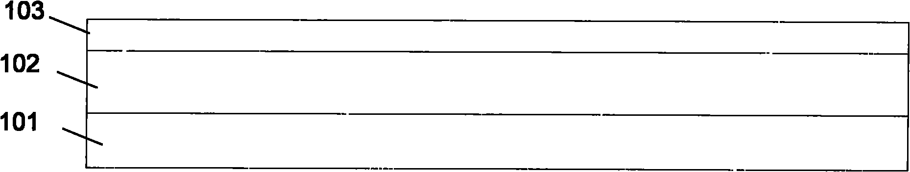
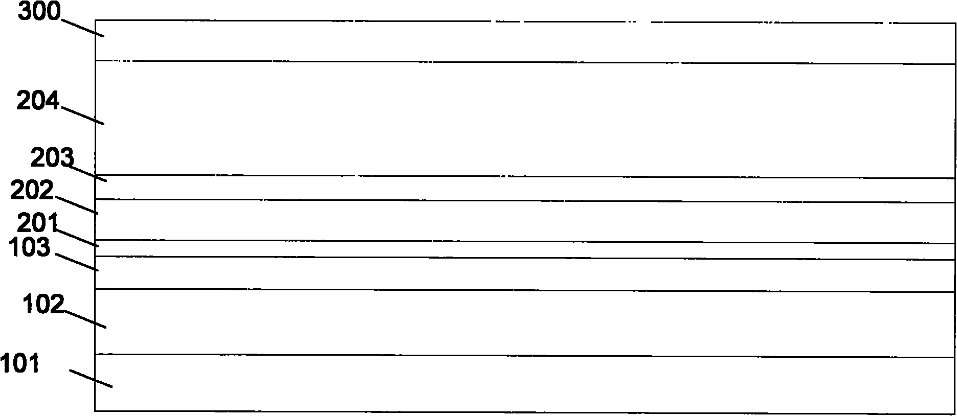
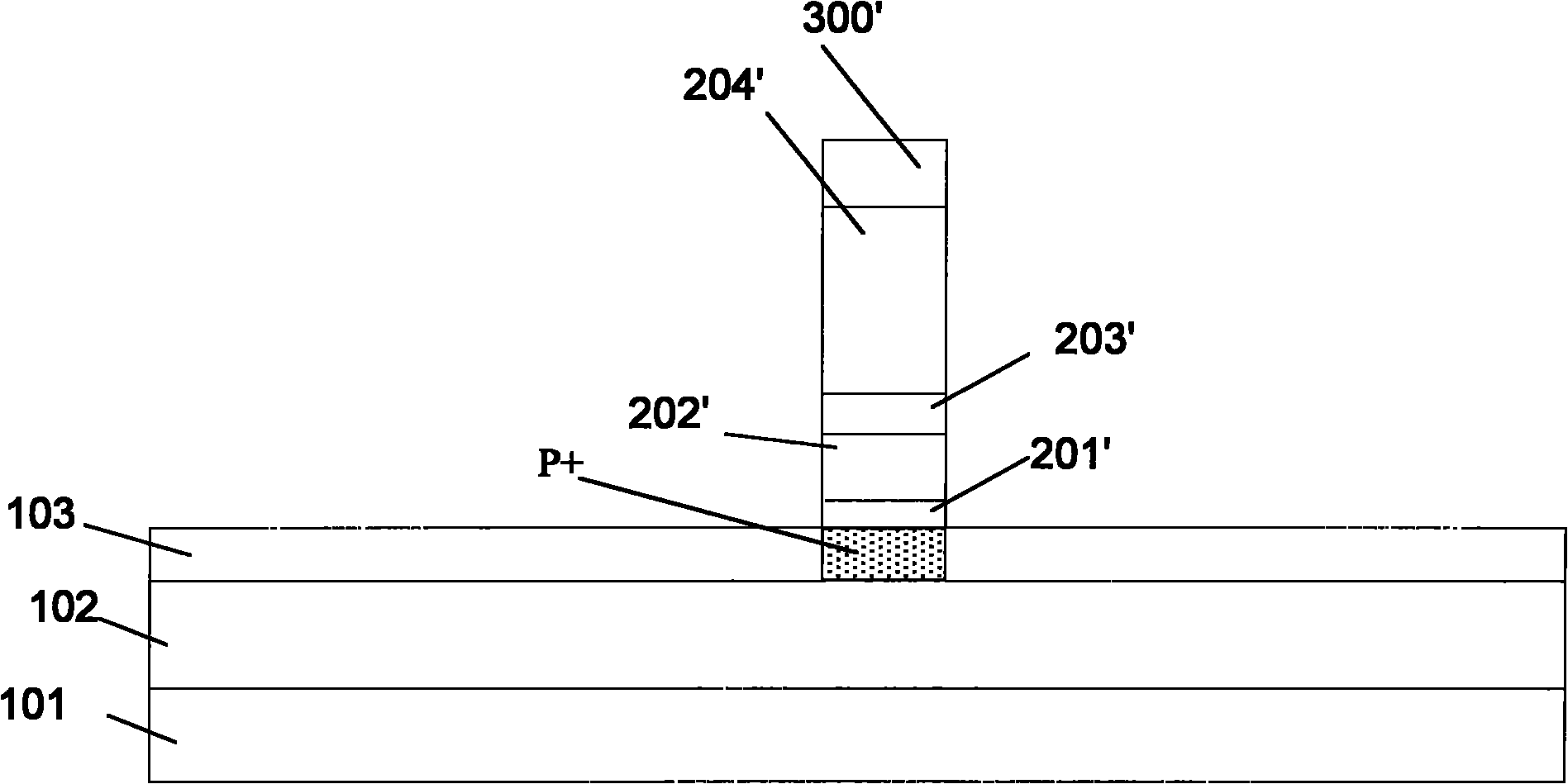
[0020] The embodiments of the present invention will be described in detail below. Examples of the embodiments are shown in the accompanying drawings, wherein the same or similar reference numerals indicate the same or similar elements or elements with the same or similar functions. The embodiments described below with reference to the accompanying drawings are exemplary, and are only used to explain the present invention, and cannot be construed as limiting the present invention.

[0021] The following disclosure provides many different embodiments or examples for implementing different structures of the present invention. In order to simplify the disclosure of the present invention, the components and settings of specific examples are described below. Of course, they are only examples, and are not intended to limit the invention. In addition, the present invention may repeat reference numbers and / or letters in different examples. This repetition is for the purpose of simplifi...


PUM


Abstract

The invention provides a semiconductor structure and a forming method thereof. The structure comprises a semiconductor substrate and a flash memory device formed on the semiconductor substrate, wherein the flash memory device comprises a channel region formed on the semiconductor substrate and a grid stack formed on the channel region, wherein the gird stack comprises a first gird dielectric layer formed on the channel region, a first conductive layer formed on the first grid dielectric layer, a second grid dielectric layer formed on the first conductive layer, a second conductive layer formed on the second grid dielectric layer, a high doping first conductive type region and a high doping second conductive type region; and the high doping first conductive type region and the high doping second conductive type region are respectively positioned at two sides of the channel region and have opposite conductive types. The invention can be used for realizing information storage of the Tunneling FET (Field Effect Transistor).

Description

Technical field [0001] The present invention relates to the technical field of semiconductor manufacturing, in particular to a TFET (Tunneling FET, tunneling field effect transistor) structure and a method of forming the same. Background technique [0002] As the size of the MOSFET (Metal Oxide Semiconductor Field Effect Transistor) continues to shrink, the traditional MOSFET structure can no longer meet the increasingly high requirements. Therefore, a TFET is proposed to meet the ever-increasing requirements of device switching performance. [0003] When a certain turn-on voltage is applied to the gate of the TFET, due to the quantum tunneling effect, the barriers on the source and drain regions on both sides of the channel region become smaller, so that the source and drain regions are quickly turned on. [0004] With the development of semiconductor technology, there is an urgent need to further reduce the turn-on voltage of the gate to meet the rapidly increasing requirements fo...

Claims


Application Information

Patent Timeline
Patent Type & Authority Applications(China)
IPC IPC(8): H01L27/115H01L29/40H01L21/8247H01L21/28
CPCH01L29/7881H01L21/28273H01L29/40114
Inventor 朱慧珑尹海洲骆志炯
Owner INST OF MICROELECTRONICS CHINESE ACAD OF SCI
Why Eureka
Try Eureka