Organic light-emitting diode display

A luminescent and display technology, applied in the field of organic electroluminescent displays, can solve problems such as damage to organic functional layers, and achieve the effects of prolonging service life, reducing distance, and simple manufacturing process

Active Publication Date: 2010-10-20
TRULY SEMICON
View PDF3 Cites 31 Cited by
  • Summary
  • Abstract
  • Description
  • Claims
  • Application Information

AI Technical Summary

Problems solved by technology

[0005] But even with the back cover and desiccant, there will still be a considerable amount of water vapor and oxygen penetrating into the OLED, damaging the organic functional layer

Method used


Image

  • Organic light-emitting diode display
  • Organic light-emitting diode display
  • Organic light-emitting diode display

Examples


Embodiment 1

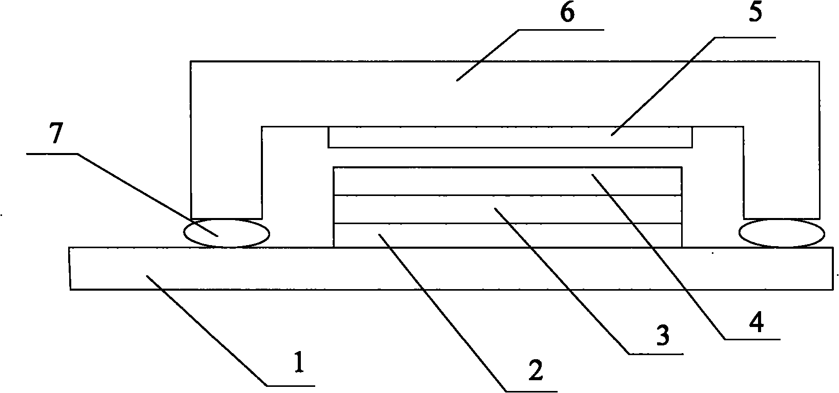
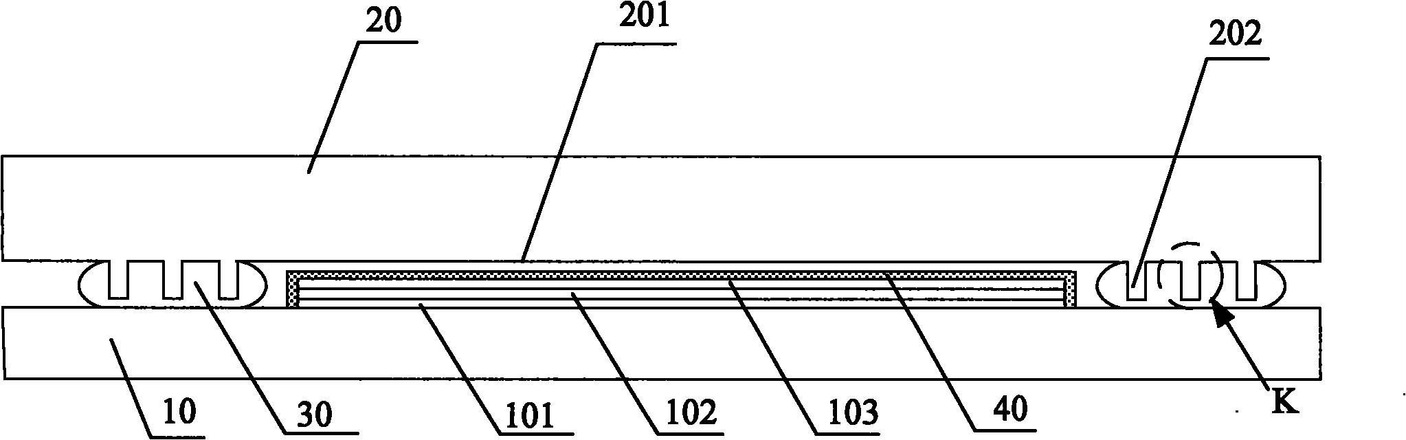
[0034] figure 2 is a schematic cross-sectional view of the OLED of the present invention. The invention provides an OLED, such as figure 2 As shown, the OLED includes: a substrate 10 , a back cover 20 , and an encapsulant 30 .

[0035] A pixel display area matrix is ​​formed on the substrate 10; each pixel display area in the pixel display area matrix includes a transparent anode 101, an organic functional layer 102 and a cathode 103 deposited on the substrate 10 in sequence. The surface of each pixel display area is covered with a water-absorbing protective layer 40; if the special conductive glass is selected for use in the preparation of the substrate 10, the pre-deposited ITO (Indium Tin Oxide, indium tin oxide) coating on the conductive glass can be used as The anode of the OLED is used.

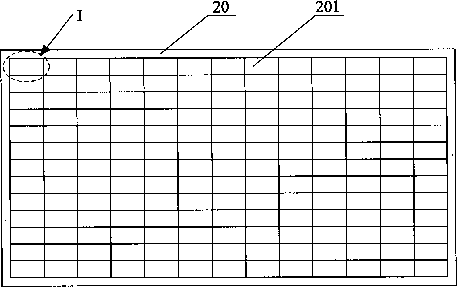
[0036] First, the rear cover of the present invention is introduced in detail. See also image 3 , Figure 4 ,in, image 3 It is a schematic bottom view of the rear cover glass...

Embodiment 2

[0053] The present embodiment provides the manufacturing method of the rear cover in the above-mentioned OLED, such as Figure 9 shown, including:

[0054] S10, forming a first pattern on a side of the rear cover glass facing the substrate.

[0055] After the back cover glass is selected, the regular polishing process will also be included. The back cover glass can be white glass with a thickness of 0.7 mm.

[0056] The first pattern covers the positions of the protrusions, and exposes the part between the light-emitting area and the protrusions. The forming of the first pattern on the back cover glass may be: spin coating photoresist on the side of the back cover glass facing the substrate, exposing and developing to form the first pattern. Wherein, the spin coating, exposure and development of the photoresist can be the same as the prior art.


PUM


Abstract

The invention discloses an organic light-emitting diode (OLED) display. The organic light-emitting diode display comprises a substrate, a rear cover and a packaging adhesive, wherein the substrate is provided with a pixel display region matrix; a water-absorbing protection layer covers the surface of each pixel display region; the surface of the rear cover facing the substrate is provided with a light emitting region corresponding to the pixel display region matrix on the substrate; the rear cover also comprises at least one ring of continuous bumps surrounding the light emitting region at the periphery of the light emitting region; and the packaging adhesive is positioned on the contact surface of the substrate and the rear cover, surrounds the light emitting region and completely covers the at least one ring of bumps surrounding the light emitting region. By forming the bumps at the periphery of the light emitting region of the rear cover, the required adhesive strength can be ensured during the packaging of the OLED, the distance between the rear cover and the substrate can be greatly reduced, and the capability of the OLED of preventing the penetration of vapor and oxygen can be enhanced; and the vapor having penetrated into the OLED can be adsorbed by further covering a transparent water-absorbing protection layer on the pixel display region, so that the organic functional layer can be protected.

Description

technical field [0001] The invention relates to the technical field of electronic appliances, in particular to an organic electroluminescence display. Background technique [0002] Organic light-emitting display (OLED, Organic Light-Emitting Diode) is an emerging flat-panel display at present, because OLED has active light emission, high contrast, can be thinned, fast response, no viewing angle limit, wide operating temperature range, low With many advantages such as power consumption, strong shock resistance and flexible display, it is recognized as the main force of the next generation of displays. [0003] The typical structure of the existing OLED is as figure 1 As shown, it includes: a substrate glass 1, an anode 2 deposited on the substrate glass 1, an organic functional layer 3 covering the anode 2, a cathode 4 located on the organic functional layer 3, a back cover 6 corresponding to the substrate glass 1, The desiccant 5 attached to the light-emitting area on the ...

Claims


Application Information

Patent Timeline
Patent Type & Authority Applications(China)
IPC IPC(8): H01L27/32H01L51/52H01L51/56
Inventor 曹绪文赵云何基强
Owner TRULY SEMICON
Why Eureka
Try Eureka