One-time programming resistance random memory unit, array, memory and operation method thereof

A technology of resistance random storage and operation method, which is applied in the field of memory, can solve the problems of large deviation in the distribution of low resistance value and high resistance value of storage resistance, difficulty in meeting the requirements of memory read and write tolerance, and achieve high read and write Tolerance, fast and accurate readout, the effect of high readout speed

Inactive Publication Date: 2010-10-27
FUDAN UNIV
View PDF6 Cites 39 Cited by
  • Summary
  • Abstract
  • Description
  • Claims
  • Application Information

AI Technical Summary

Problems solved by technology

[0012] Due to the stability of the storage material of binary or more than binary multi-element metal oxides, the deviation of the manufacturing process, etc., the distribution deviation of the low resistance value and the high resistance value of the storage resistor is relatively large, and the low resistance value and the high resistance value are relatively large. The difference between the high-resistance resistance values ​​tends to decrease with the increase of the array or the extension of the storage time and the increase of the number of r

Method used


Image

  • One-time programming resistance random memory unit, array, memory and operation method thereof
  • One-time programming resistance random memory unit, array, memory and operation method thereof
  • One-time programming resistance random memory unit, array, memory and operation method thereof

Examples


Embodiment 1

[0043] Where the referenced figures are schematic illustrations of idealized embodiments of the invention, the illustrated embodiments of the invention should not be construed as limited to the specific shapes of the regions shown in the figures.

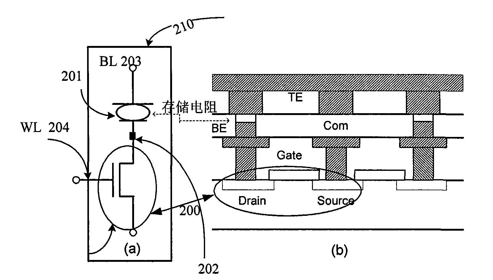
[0044] Figure 4 It is a schematic diagram of the circuit structure of the one-time programming resistance random memory unit provided by the present invention. Such as Figure 4 As shown, two one-time programming RRAM cells 420 and 410 are included. Taking the one-time programming RRAM unit 420 as an example, it includes a first storage resistor 401, a first gate transistor 411 connected in series with the first storage resistor, a second storage resistor 402, and a second transistor connected in series with the first storage resistor. Strobe tube 412 . In this embodiment, one end of the first storage resistor 401 is connected in series with the first gate transistor 411, and the other end is also connected with the bit line BL1...

Embodiment 2

[0053] Figure 5 A schematic diagram of the circuit structure of the one-time programming resistance random access memory array provided by the present invention. It should be understood that in actual implementation, the number of rows and columns of the storage array can be changed according to needs, which is only described as M rows and N columns for the convenience of description here. as shown in the picture Figure 5 As shown, the memory array includes M rows×N columns of one-time programming resistance random access memory cells, the first row of the one-time programming resistance random access memory array includes memory cells 551, 552, to 55N, and each memory cell is a basic unit of the memory array , the storage unit 551 includes a first storage resistor 501, a second storage resistor 502, a first gate transistor 511, and a second gate transistor 512, and its structure is the same as that of Figure 4 The described embodiments are essentially the same. WL 1 to...

Embodiment 3

[0059] Figure 7 Shown is a schematic circuit diagram for operating the one-time programming RRAM array provided by the present invention. Such as Figure 7 As shown, its storage array structure is the same as Figure 5 It is the same as shown, but the erasing and programming and reading circuit parts for operation are added. Erasing, programming, and reading circuits are composed of the following parts: column decoder 602, row decoder 603, write drive circuit 607, sense amplifier 606, input and output buffer 608, data control signal 750, data selection transfer transistor 751 , 752, inverter 753, erase control transmission tubes 761, 763, programming control transmission tubes 762, 765, and read control transmission tube 764. The specific operation method of the storage array provided by the present invention will be described in detail below.

[0060] First, the erase method

[0061] The memory array needs to be erased before it is delivered to the user for programming,...


PUM


Abstract

The invention belongs to the technical field of the memory, and relates to a one-time programming resistance random memory unit, an array, a memory and an operation method thereof. The one-time programming resistance random memory unit utilizes binary or multi-variant metal oxide which has the structural characteristic of 2T2R, and represents the memory state 1 and 0 through the state combination difference of a first memory resistance and a second memory resistance. The one-time programming resistance random memory unit, array and memory are not easy to be influenced by the process deviation, and have the advantages of fast reading speed, high read-write tolerance and nonvolatility.

Description

technical field [0001] The invention belongs to the technical field of memory, and relates to a technology of a one-time programming resistance random memory cell using metal oxide as a storage resistor, in particular to a one-time programming resistance random memory cell including a 2T2R structure, a memory array, a memory and a storage operation method thereof . Background technique [0002] The non-volatile memory can still maintain the stored data when the power is off, which makes the non-volatile memory have extremely wide applications in various types of electronic devices. One-time-programmable memory (OTP) is one of the common non-volatile memories. It stores logic information through memory cells crossed by word lines and bit lines. Among them, common memory cells include fuses, antifuse and charge trapping Devices (such as floating gate avalanche injection field effect transistors). Program-once memory is generally not reprogrammable. [0003] For fuse and ant...

Claims


Application Information

Patent Timeline
IPC IPC(8): G11C17/14
Inventor 林殷茵金钢尹明张佶吴雨欣解玉凤
Owner FUDAN UNIV
Why Eureka
Try Eureka