Rectifying device for cross array structure memory

A rectifier device and cross-array technology, applied in the field of microelectronics manufacturing and memory, to achieve the effects of facilitating integration, suppressing read crosstalk, and reducing impact

Active Publication Date: 2012-09-05
INST OF MICROELECTRONICS CHINESE ACAD OF SCI
View PDF0 Cites 0 Cited by
  • Summary
  • Abstract
  • Description
  • Claims
  • Application Information

AI Technical Summary

Problems solved by technology

However, the performance index based on the diode in the 1D1R structure has always been a very difficult problem in the research of new memory.
Based on the 32nm technology node, if the reset (Reset) current of the memory cell is 10 microamps, the current density of the required diode is as high as 10 microamps. 6 A / cm 2 , while the current density of rectifier diodes reported for memory cells is only 10 4 A / cm 2

Method used


Image

  • Rectifying device for cross array structure memory
  • Rectifying device for cross array structure memory
  • Rectifying device for cross array structure memory

Examples


Embodiment Construction

[0033] In order to make the object, technical solution and advantages of the present invention clearer, the present invention will be described in further detail below in conjunction with specific embodiments and with reference to the accompanying drawings.

[0034] Figures 5 to 6 is a schematic diagram illustrating an embodiment of the present invention.

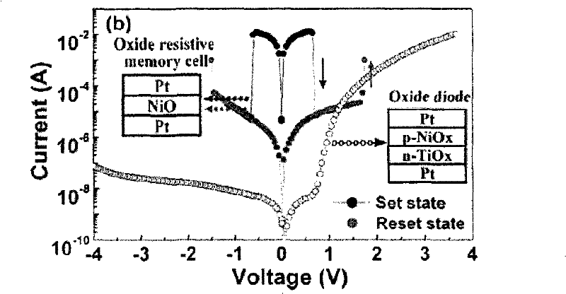
[0035] Figure 5 Yes is actually made Pt / ZrO 2 :Au / n + Schematic diagram of the structure of a Si rectifier diode device. Au nanocrystals 503 are obtained through the N 2 Annealed at 800°C in atmosphere.

[0036] In one embodiment of the present invention, with n + Type silicon was used as the substrate, and Au nanocrystal-doped ZrO with a thickness of 50nm was deposited by electron beam evaporation process. 2 As a functional layer film, then at 800°C N 2 Annealing was carried out for 2 minutes in an atmosphere, and then a 50nm-thick Pt upper electrode layer was deposited. The fabrication of the rectifier diode de...


PUM


Abstract

The invention relates to the technical field of microelectronic devices and memories, and discloses a rectifying device compatible with a CMOS process for a cross array structure memory. The rectifying device comprises an upper electrode, a lower electrode and a functional layer film between the upper electrode and the lower electrode. The rectifying device can provide higher current density, andthe rectifying device is connected in series with a memory device to form a 1D1R structure which can inhibit the crosstalk phenomenon in the cross array structure memory. The rectifying device for the cross array structure memory has the advantages of simple structure, easy integration and low cost, and is favorable for wide popularization and application.

Description

technical field [0001] The invention belongs to the technical field of microelectronics manufacturing and memory, and in particular relates to a rectifying device used in memory with a cross-array structure. Background technique [0002] Memory can be roughly divided into two categories: volatile memory and nonvolatile memory. Volatile memory immediately loses the stored information when the power is turned off; it requires continuous power supply to maintain data, represented by SRAM and DRAM. Non-volatile memory, its main feature is that it can keep stored information for a long time without power on, currently the most used non-volatile memory is flash memory (Flash). With the demand for large-capacity and low-power storage in multimedia applications and mobile communications, non-volatile memory, especially flash memory (Flash), has become larger and larger in the market share of semiconductor devices. Become a very important memory type. [0003] Although flash memor...

Claims


Application Information

Patent Timeline
Patent Type & Authority Patents(China)
IPC IPC(8): H01L27/24H01L45/00G11C13/00
Inventor 刘明左青云龙世兵
Owner INST OF MICROELECTRONICS CHINESE ACAD OF SCI
Why Eureka
Try Eureka