Eureka AIR delivers breakthrough ideas for toughest innovation challenges, trusted by R&D personnel around the world.

Oxide semiconductor device including insulating layer and display apparatus using the same

A technology for oxide semiconductors and display devices, which is applied to semiconductor devices, transistors, electrical components, etc., to achieve the effect of suppressing the reduction of resistance and high productivity

Inactive Publication Date: 2010-11-10
CANON KK
View PDF8 Cites 50 Cited by
  • Summary
  • Abstract
  • Description
  • Claims
  • Application Information

AI Technical Summary

Problems solved by technology

Therefore, a display device using an oxide semiconductor device manufactured by a low-temperature process has not yet been put into practical use

Method used


Image

  • Oxide semiconductor device including insulating layer and display apparatus using the same
  • Oxide semiconductor device including insulating layer and display apparatus using the same
  • Oxide semiconductor device including insulating layer and display apparatus using the same

Examples


Embodiment Construction

[0038] Hereinafter, an oxide semiconductor device including an insulating layer and a display device using the oxide semiconductor device according to the present invention will be described in detail with reference to the accompanying drawings.

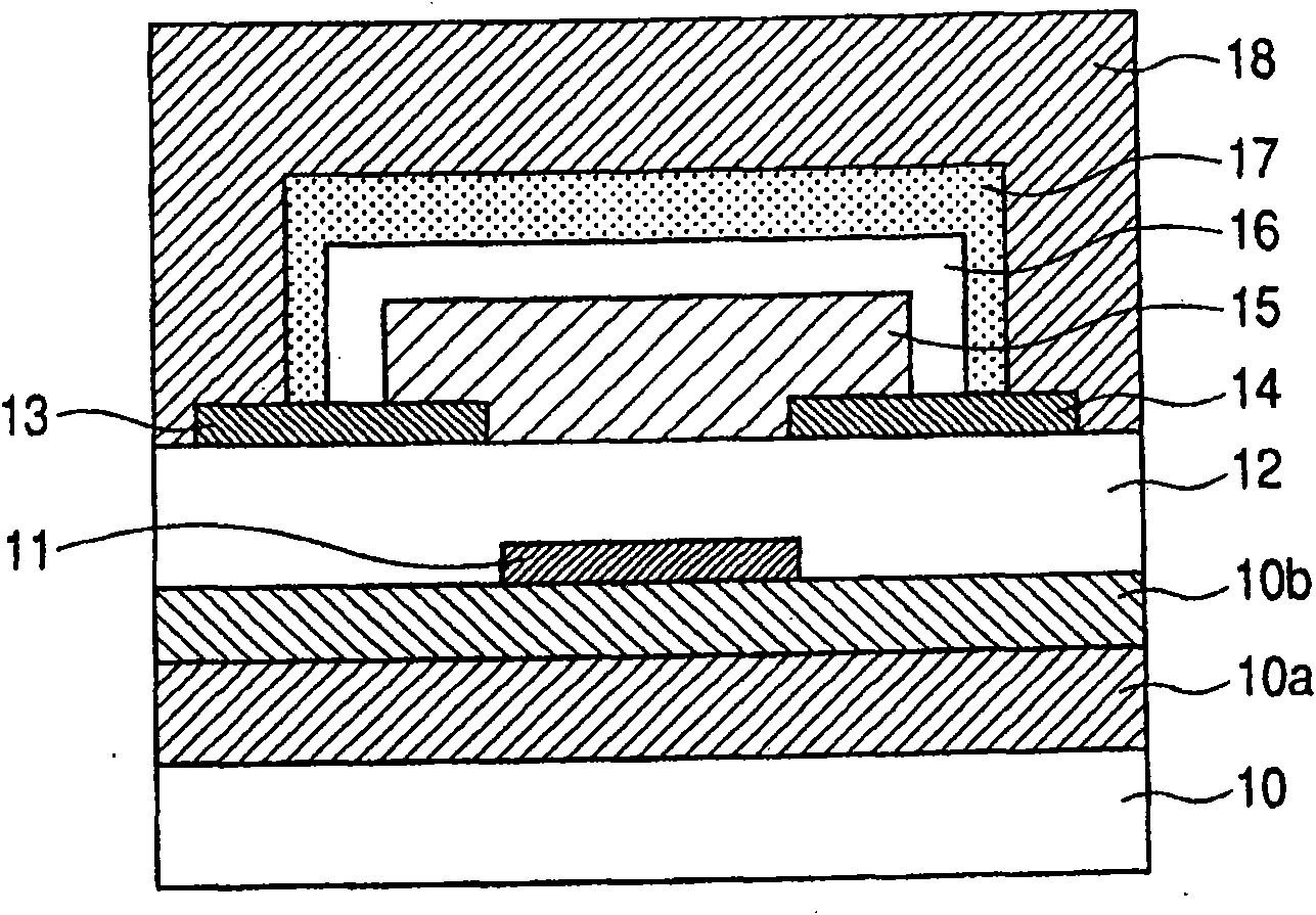
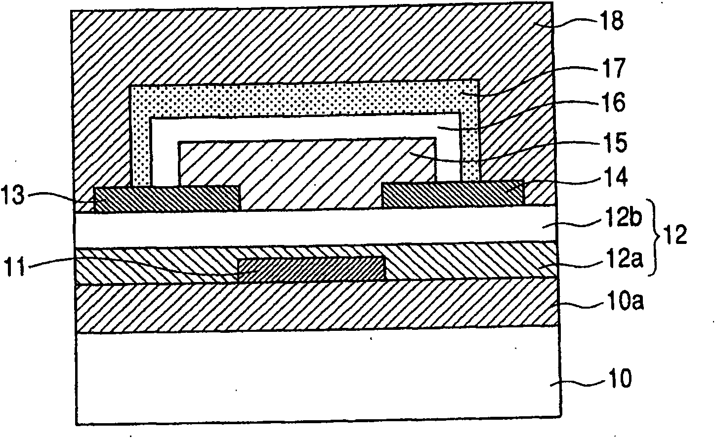
[0039] Figure 1A and Figure 1B A structural example of a bottom-gate / bottom-contact type field effect transistor as a representative oxide semiconductor device including an insulating layer structure according to the present invention is shown.

[0040] Figure 1A A substrate 10, a third insulating layer 10a serving as a barrier coating, a second insulating layer 10b, a gate electrode 11, a first insulating layer 12 serving as a gate insulating layer, a source electrode 13, a drain electrode 14, an oxide semiconductor layer 15, a first insulating layer 16 serving as a protective layer, a second insulating layer 17 serving as a protective layer, and a third insulating layer 18 serving as a protective layer.

[0041] Figure 1B Sho...


PUM


Abstract

Provided is an oxide semiconductor device including an oxide semiconductor layer and an insulating layer coming into contact with the oxide semiconductor layer in which the insulating layer includes: a first insulating layer coming into contact with an oxide semiconductor, having a thickness of 50 nm or more, and including an oxide containing Si and O; a second insulating layer coming into contact with the first insulating layer, having a thickness of 50 nm or more, and including a nitride containing Si and N; and a third insulating layer coming into contact with the second insulating layer, the first insulating layer and the second insulating layer having hydrogen contents of 4 x 10²¹ atoms / cm3 or less, and the third insulating layer having a hydrogen content of more than 4 x 10²¹ atoms / cm3.

Description

technical field [0001] The present invention relates to oxide semiconductor devices. More particularly, the present invention relates to an oxide semiconductor device including an insulating layer, and to a display device as an application example of the oxide semiconductor device. Background technique [0002] In recent years, a thin film transistor (TFT) having a channel layer of a transparent conductive oxide polycrystalline thin film containing zinc oxide (ZnO) as a main component has been actively developed (Japanese Patent Application Laid-Open No. 2002-076356). [0003] Transparent conductive oxide polycrystalline thin films can be formed at low temperatures and are transparent to visible light, whereby flexible transparent TFTs can be formed on substrates such as plastic plates or films. [0004] However, an oxide semiconductor including ZnO has high sensitivity to the atmosphere, and thus, in order for the oxide semiconductor to be practically used as a semiconduct...

Claims


Application Information

Patent Timeline
Patent Type & Authority Applications(China)
IPC IPC(8): H01L29/786
CPCH01L29/78606H01L29/4908H01L29/7869
Inventor 佐藤步林亨薮田久人渡边智大
Owner CANON KK
Why Eureka
Eureka Blog
Learn More