
Semiconductor element and manufacturing method thereof

A manufacturing method, semiconductor technology, applied in the direction of semiconductor/solid-state device manufacturing, semiconductor devices, electrical components, etc., can solve the problems of reducing the effect of carrier mobility improvement, general products without suitable structure, stress layer far away from the channel region, etc. , achieve the effect of alleviating the hot carrier effect, enhancing electron mobility, and reducing overlapping capacitance

Active Publication Date: 2013-01-02
MACRONIX INT CO LTD
View PDF0 Cites 0 Cited by
  • Summary
  • Abstract
  • Description
  • Claims
  • Application Information

AI Technical Summary

Problems solved by technology

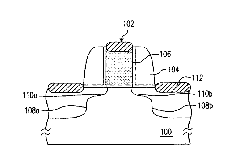
In addition, when a stress layer is formed on the substrate 100, the thick spacer 104 tends to cause the stress layer to be far away from the channel region, thus reducing the effect of the stress layer on carrier mobility.
[0005] It can be seen that the above-mentioned existing semiconductor element and its manufacturing method obviously still have inconvenience and defects in structure and use, and need to be further improved urgently.
In order to solve the above-mentioned problems, the relevant manufacturers have tried their best to find a solution, but no suitable design has been developed for a long time, and the general products do not have a suitable structure to solve the above-mentioned problems. How to effectively ensure the semiconductor components Reliability of components, and improving the performance of semiconductor components, this is obviously a problem that the relevant industry is eager to solve

Method used


Image

  • Semiconductor element and manufacturing method thereof
  • Semiconductor element and manufacturing method thereof
  • Semiconductor element and manufacturing method thereof

Examples


experiment example

[0103] Image 6 Illustrated are the lateral electric field distribution curves corresponding to different positions in the channel region parallel to the first surface of the NMOS according to the prior art and the NMOS of the experimental example of the present invention.

[0104] like Image 6 As shown, the lateral electric field distributions of the conventional NMOS and the NMOS proposed by the present invention in the channel region near the interface between the gate structure and the silicon substrate are simulated respectively. The gate length of the conventional NMOS and the NMOS of the experimental example of the present invention is about 90 nm. When the same bias voltage is respectively applied to the two elements, the lateral electric field distribution of the conventional NMOS is much higher than the lateral electric field distribution of the NMOS of the experimental example of the present invention. Since the lateral electric field significantly affects the ho...


PUM


Abstract

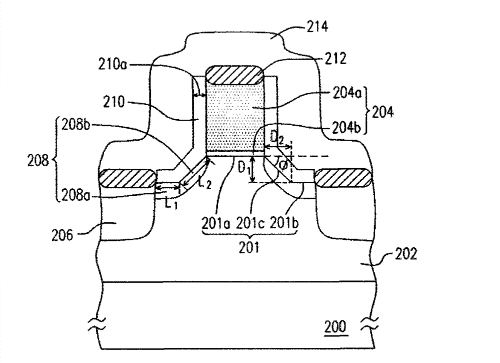
The invention relates to a semiconductor element and a manufacturing method thereof. The semiconductor element comprises a base, a grid structure, doped zones and soft doped zones. The base has a step-shaped upper surface, wherein the step-shaped upper surface comprises a first surface, a second surface and a third surface; the second surface is lower than the first surface; the third surface is connected to the first and the second surfaces; the grid structure is arranged on the first surface; the doped zones are arranged in the base at two sides of the grid structure and located below the second surface; the soft doped zones are respectively arranged in the base between the grid structure and the doped zones, and each soft doped zone comprises a first part and a second part which are connected to each other, wherein the first part is arranged below the second surface and the second part is arranged below the third surface. The semiconductor element employs the inclined and bent softdoped zones as a source electrode and a drain electrode for extending, beneficial to lightening hot carrier effect without reducing dopant concentration of the soft doped zones, and capable of decreasing leakage current of the drain electrode caused by the grid and overlap capacitance between the grid and the drain electrode.

Description

technical field [0001] The present invention relates to a semiconductor element and a manufacturing method thereof, in particular to a metal oxide semiconductor (MOS) transistor and a manufacturing method thereof. Background technique [0002] With the rapid development of semiconductor manufacturing process technology, in order to improve the speed and performance of the components, the size of the entire circuit components must be continuously reduced, and the integration level of the components must be continuously improved. Under the trend of higher and higher requirements for component integration, changes in component characteristics such as leakage current, hot carrier effect (hot carrier effect) or short channel effect (SCE) must be considered. Avoid serious impact on the reliability and performance of integrated circuits. [0003] Taking metal oxide semiconductor transistors as an example, figure 1 It is a schematic cross-sectional view of a conventional metal-oxi...

Claims


Application Information

Patent Timeline
Patent Type & Authority Patents(China)
IPC IPC(8): H01L29/78H01L29/38H01L21/336
Inventor 杨怡箴吴冠纬张耀文卢道政
Owner MACRONIX INT CO LTD
Learn More