

Top gate metal oxide thin film transistor switching device for imaging applications
a technology of metal oxide thin film transistor and switching device, which is applied in the direction of radiation control devices, semiconductor devices, electrical apparatus, etc., can solve the problems of inability to meet the needs of imaging applications, etc., to achieve simple process flow, reduce processing costs, and fast switching speed
- Summary
- Abstract
- Description
- Claims
- Application Information
AI Technical Summary
Benefits of technology
Problems solved by technology
Method used
Image

Examples
Embodiment Construction
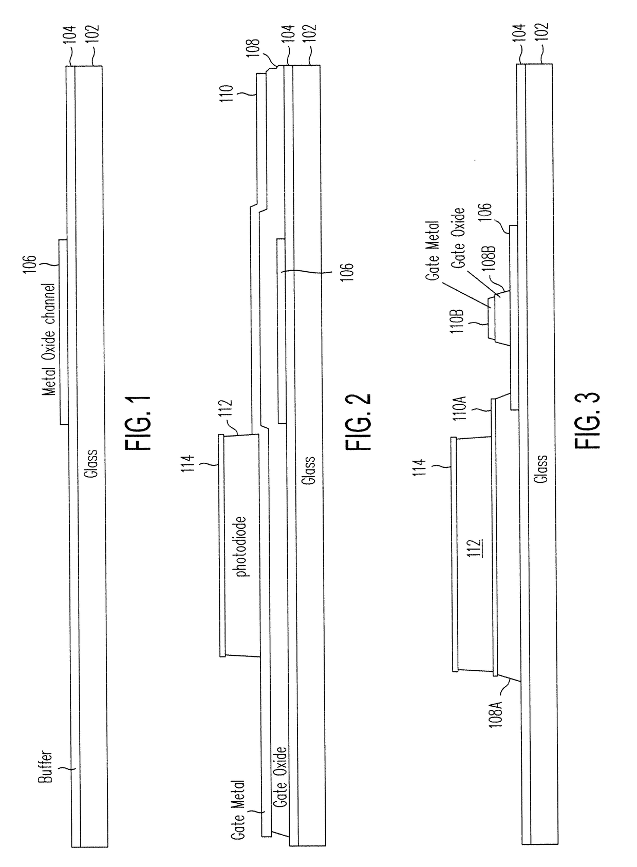
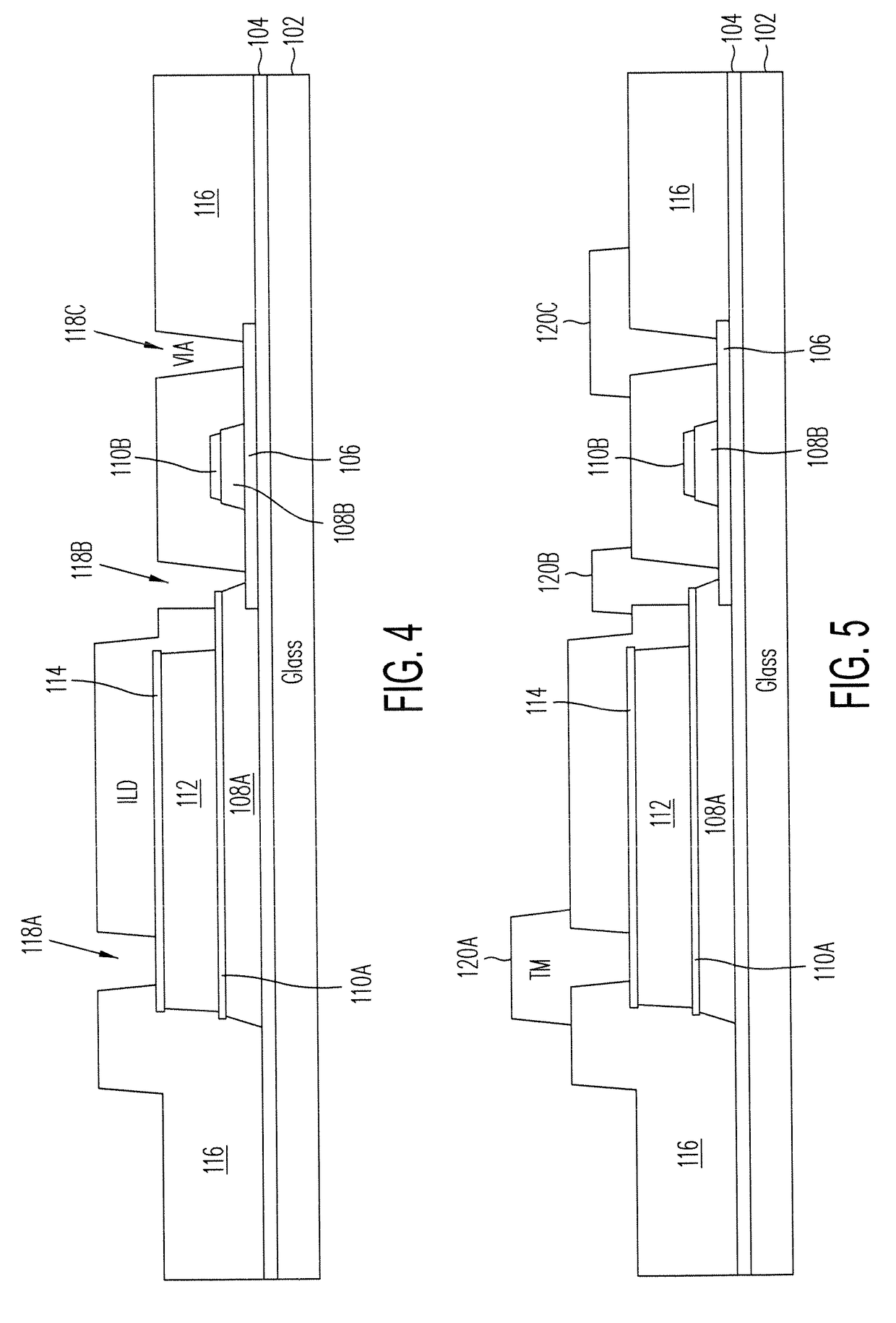
[0014]A manufacturing process for an image sensor device performed is illustrated with respect to FIGS. 1-6.
[0015]Referring to FIG. 1, a buffer dielectric film 104 is deposited on a substrate 102 using PECVD. A metal oxide channel film 106 is deposited by a PVD system and patterned using a photolithography process. Substrate 102 can comprise a glass, plastic, metal foil, or silicon substrate. The buffer layer 104 can comprise a silicon dioxide, silicon nitride, silicon oxynitride, or alumina dielectric film. The metal oxide channel 106 can comprise a patterned Indium oxide (whose composition varies, but major composition components are Indium, Zinc, Gallium, Hafnium, Aluminum, or Indium-Zinc-Gallium-Oxide (IGZO)) layer.
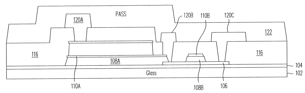
[0016]Referring to FIG. 2, a gate oxide layer 108, a gate metal layer 110, a photodiode stack film including photodiode layer 112 and top contact layer 114 are deposited using PECVD and PVD. The photodiode layers 112 and 114 are patterned using an etch process. The ga...
PUM
| Property | Measurement | Unit |
|---|---|---|
| transparent | aaaaa | aaaaa |
| Transparent | aaaaa | aaaaa |
| electrical behavior | aaaaa | aaaaa |
Abstract
Description
Claims
Application Information