Source/drain profile engineering for enhanced p-MOSFET

Active Publication Date: 2016-08-16
GLOBALFOUNDRIES US INC
View PDF6 Cites 4 Cited by
  • Summary
  • Abstract
  • Description
  • Claims
  • Application Information

AI Technical Summary

Benefits of technology

This patent describes a type of semiconductor device called a pMOSFET. These pMOSFETs have several advantages over previous designs, including reduced overlap capacitance, reduced junction leakage, and good overall electrical performance. These methods provide better performance in semiconductor devices and help them to achieve more reliable and efficient results.

Problems solved by technology

As devices scale smaller, shrinking design and demand for doping in the source / drain in p-type MOSFET's lead to increased overlap capacitance.
Since high overlap capacitance compromises device alternating current (AC) performance, the scaling of semiconductor devices and components, such as MOSFET's, presents a challenge to fabricating high-quality nano / micron-scale components with good electrical performance.

Method used


Image

  • Source/drain profile engineering for enhanced p-MOSFET
  • Source/drain profile engineering for enhanced p-MOSFET
  • Source/drain profile engineering for enhanced p-MOSFET

Examples


examples

[0063]The invention will now be illustrated, but not limited, by reference to the specific embodiments described in the following examples.

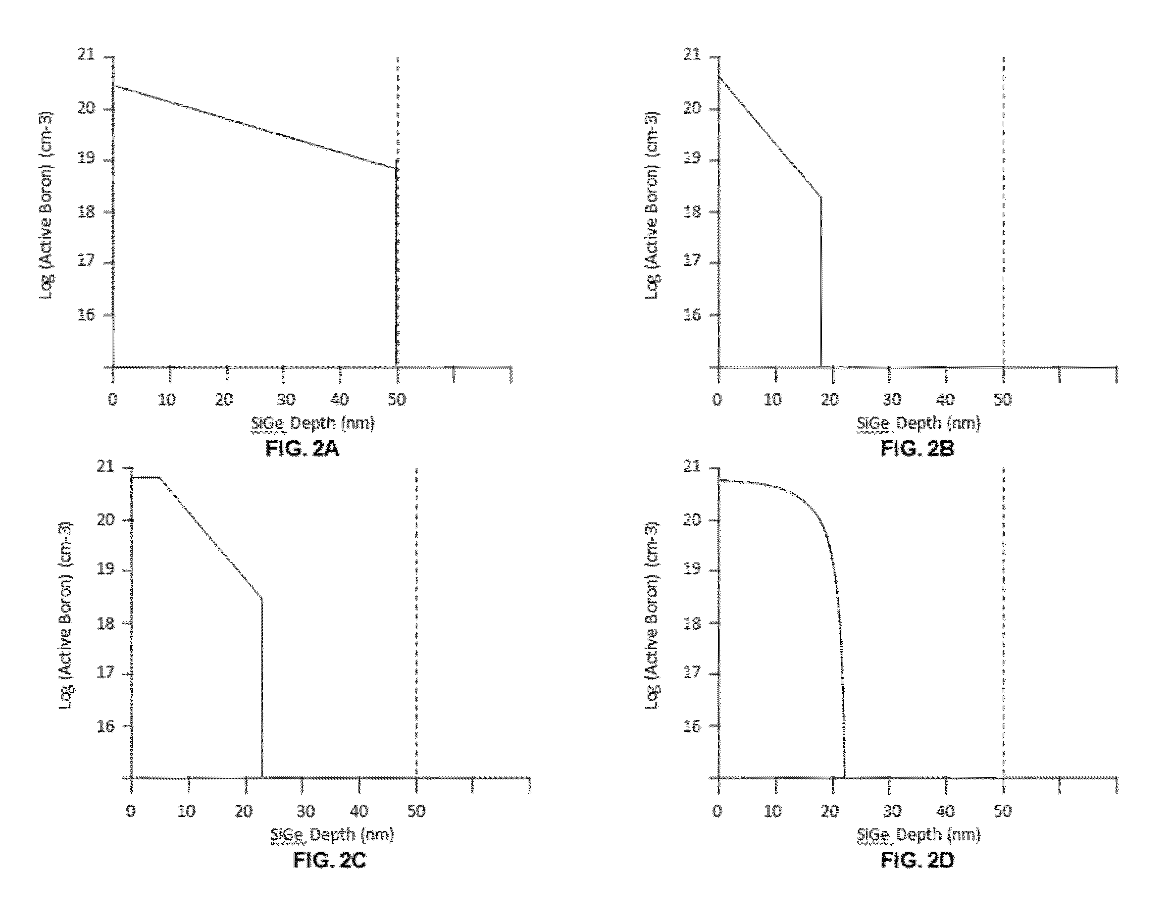
[0064]Simulation testing is done using a well calibrated deck for 20 nm technology. The simulation is based on pMOSFET's having a 50 nm thick SiGe film, where L1 (the initially-deposited SiGe) is about 20 nm thick, and L2 (the upper portion of the SiGe) is about 30 nm thick. Common parameters are shared for all testing, except that SiGe films have different boron doping profiles. FIG. 5 is a chart that illustrates the final boron doping profiles from the simulation testing. Referring to the x axis of the chart in FIG. 5 (which provides depth (or width), in micron×10−2), the SiGe film width spans from 0.00 (which represents the SiGe upper surface) to 5.00, which represents the lower interface of the SiGe, which is in contact with a semiconductor substrate. The area to the left of 0.00 represents the contact region of the pMOSFET. The y axis in FIG...


PUM


Abstract

P-type metal-oxide semiconductor field-effect transistors (pMOSFET's), semiconductor devices comprising the pMOSFET's, and methods of forming pMOSFET's are provided. The pMOSFET's include a silicon-germanium (SiGe) film that has a lower interface in contact with a semiconductor substrate and an upper surface, and the SiGe film has a graded boron doping profile where boron content increases upwardly over a majority of the width of boron-doped SiGe film between the lower interface of the SiGe film and the upper surface of the SiGe film. Methods of forming the pMOSFET's include: providing a semiconductor substrate; depositing a SiGe film on the semiconductor substrate, thereby forming a lower interface of the SiGe film in contact with the semiconductor substrate, and an upper surface of the SiGe film; and doping the SiGe film with boron to form a SiGe film having a graded boron doping profile where boron content increases upwardly over a majority of the width of boron-doped SiGe film between the lower interface of the SiGe film and the upper surface of the SiGe film.

Description

FIELD OF THE INVENTION[0001]The present invention generally relates to p-type metal-oxide semiconductor field-effect transistors (pMOSFET's), to semiconductor devices that include the pMOSFET's, and to methods of forming pMOSFET's.BACKGROUND OF THE INVENTION[0002]Integrated circuits are formed from semiconductor substrates within and upon whose surfaces may be formed resistors, transistors, diodes and other electrical circuit elements. As described by Moore's law, the semiconductor industry drives down pattern dimensions in order to reduce transistor size and enhance processor speed at a rapid pace.[0003]As devices scale smaller, shrinking design and demand for doping in the source / drain in p-type MOSFET's lead to increased overlap capacitance. Since high overlap capacitance compromises device alternating current (AC) performance, the scaling of semiconductor devices and components, such as MOSFET's, presents a challenge to fabricating high-quality nano / micron-scale components with ...

Claims


Application Information

Patent Timeline
IPC IPC(8): H01L21/22H01L21/02H01L29/66H01L29/16H01L29/78H01L29/36
CPCH01L29/365H01L29/16H01L29/78H01L21/02532H01L21/02579H01L29/66477H01L29/105H01L29/1054H01L29/66568
Inventor MISHRA, SHIV KUMARLI, ZHIQINGBEASOR, SCOTTPANDEY, SHESH MANI
Owner GLOBALFOUNDRIES US INC
Why Eureka
Try Eureka