

Polysilicon selective emitter solar cell manufacture process
A solar cell and manufacturing process technology, applied in sustainable manufacturing/processing, final product manufacturing, circuits, etc., can solve problems such as high cost, complicated process, and impact on material quality, and achieve high production efficiency, simple process, and energy efficiency. The effect of low consumption
- Summary
- Abstract
- Description
- Claims
- Application Information
AI Technical Summary
Problems solved by technology
Method used
Image

Examples
Embodiment Construction
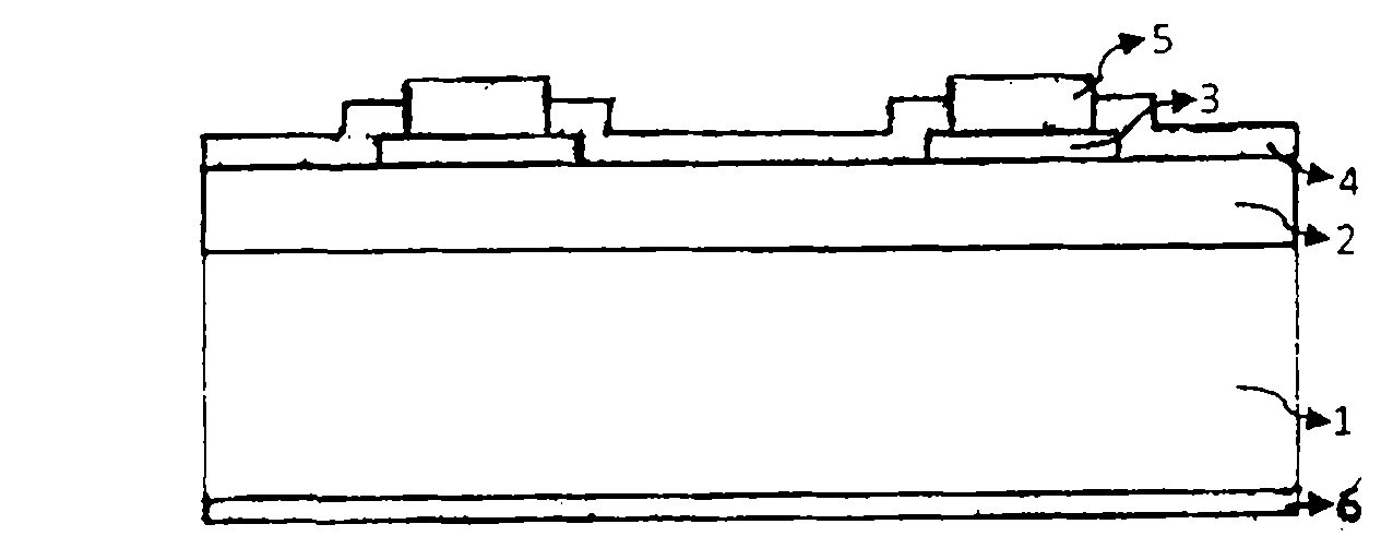
[0020] like figure 1 A polysilicon selective emitter solar cell using wet chemical etch-back is shown, including polysilicon wafer 1 and silicon wafer 1 diffused and junctioned to form a low-concentration phosphorus-doped region 2, and the front metallized electrode region 5 below The local high-concentration phosphorus doping region 3 .
[0021] The schematic cross-sectional view of the solar cell continuous process steps adopting the process of the present invention is as follows Figure 2 to Figure 6 ;
[0022] The specific steps are as follows:
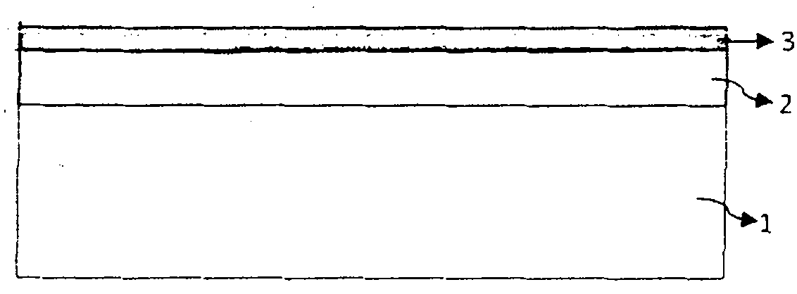
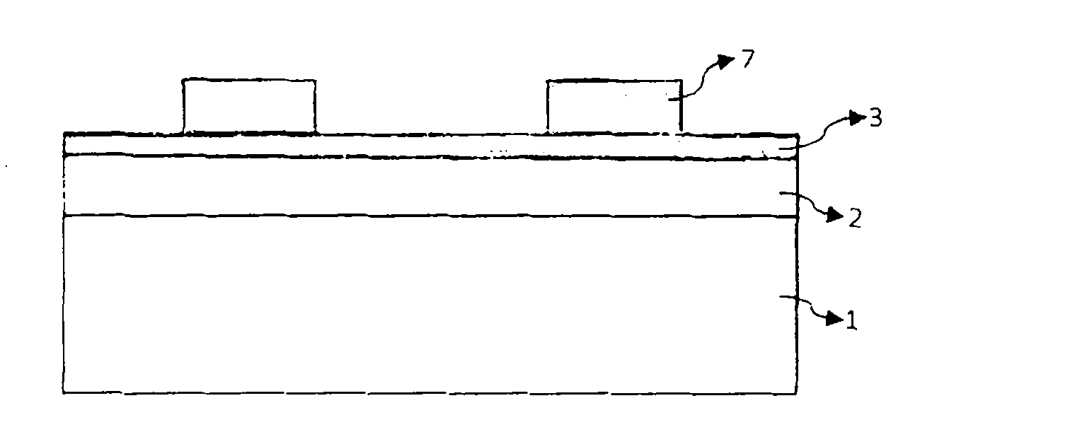
[0023] After the polycrystalline silicon wafer is dedamaged and textured (conventional method), it is diffused in a tubular diffusion furnace (conventional method), such as figure 2 As shown, the low-concentration phosphorus-doped region 2 and the high-concentration phosphorus-doped region 3 are completed in the same diffusion process. On the emitter, according to the front metallization pattern area 5, the etch-back barrier ...
PUM
 Abstract
Description
Claims
Application Information