Manufacturing method for reducing area of SONOS storage unit

A technology for memory cells and manufacturing methods, which is applied in semiconductor/solid-state device manufacturing, electrical components, and photoplate-making process coating equipment, etc., and can solve problems such as minimum distance process limitations, breakdown failure, and lateral etching of the insulating oxide layer 2 , to achieve the effect of reducing lateral etching, shrinking spacing, and reducing unit area

Active Publication Date: 2010-12-22
SHANGHAI HUAHONG GRACE SEMICON MFG CORP
View PDF0 Cites 4 Cited by
  • Summary
  • Abstract
  • Description
  • Claims
  • Application Information

AI Technical Summary

Problems solved by technology

[0011] In step 6) due to the isotropic principle of wet etching, the insulating oxide layer 2 in the SONOS region is worse than that of the nitride layer 3 and the tunnel oxide layer 4 due to the adhesion with the antireflection layer 7 or photoresist 8 Many, it will cause lateral etching of the insulating oxide layer 2, and then when the gate is formed, the gate of the SONOS tube must be formed in the area where the insulating oxide layer 2 remains, because the insulating oxide layer 2 is an insulating layer. If there is no such layer, the device It will directly break down and fail, so it is restricted by the lateral etching of the insulating oxide layer 2, and the minimum distance between the SONOS tube and the ordinary transistor is limited by the process

Method used


Image

  • Manufacturing method for reducing area of SONOS storage unit
  • Manufacturing method for reducing area of SONOS storage unit
  • Manufacturing method for reducing area of SONOS storage unit

Examples


Embodiment Construction

[0033] The present invention will be described in further detail below in conjunction with the accompanying drawings and embodiments.

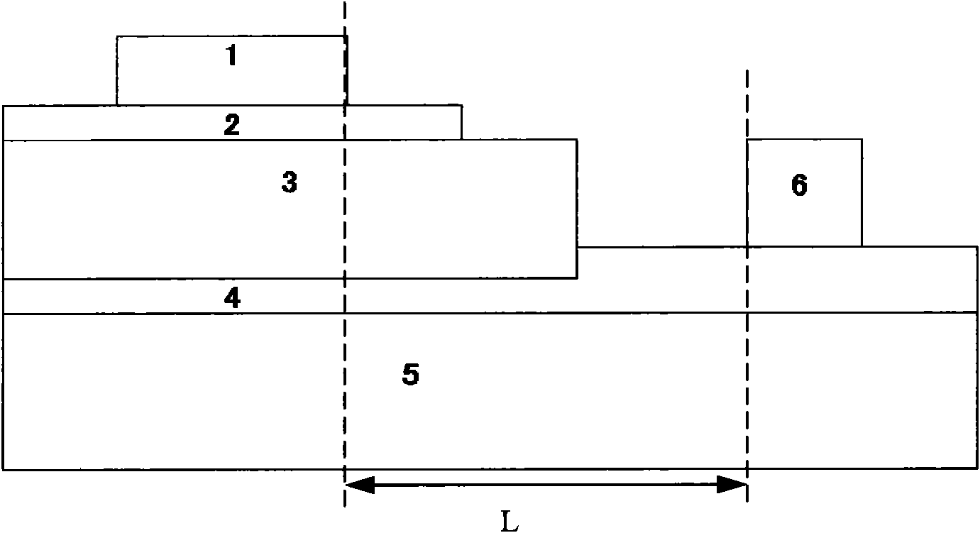
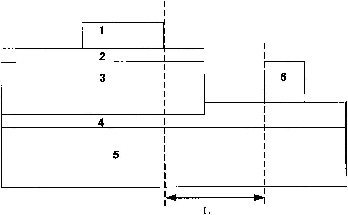
[0034] As shown in Figure 5, the present invention provides a kind of manufacturing method of SONOS memory, and its processing step is:

[0035] 1) on silicon substrate 5, SiO2 is fully deposited to form SiO2 layer 4, see Figure 5A ; For devices with an operating voltage of less than 15V, the thickness is 50-250 angstroms, and the growth method is usually thermal growth or PVD, CVD deposition.

[0036] 2) Photolithography removes the SiO2 in the SONOS tube area, and forms a SiO2 protective layer (anti-reflection barrier layer 8 and photoresist 7) ​​in other areas (ie, the common transistor area), see Figure 5B ; Etching generally uses wet etching containing HF liquid.

[0037] 3) Fully deposit ONO three-layer film (Oxide-Nitride-Oxide, insulating oxide layer 2-nitride layer 3-tunnel oxide layer 4), see Figure 5C ; For devices with an ope...


PUM

PropertyMeasurementUnit
thicknessaaaaaaaaaa

Abstract

The invention discloses a manufacturing method for reducing an area of an SONOS storage unit, comprising the following steps: (1) completely depositing SiO2 on a silicon substrate; (2), removing SiO2 in an SONOS pipe zone by photoetching and etching, and forming a SiO2 protective layer in a common transistor zone; (3) completely depositing an ONO three-layer film; (4) protecting the ONO zone of the SONO pipe by photoetching, and forming a SiO2 protective layer on the zone; (5) removing ON in the common transistor zone by dry etching; (6) carrying out heating on silicon wafers; (7) removing the rest of SiO2 in the common transistor zone by wet etching; and (8) forming a gate oxide and a grid electrode in the follow-up steps. The method can reduce horizontal etching of SiO2 on the upper layer of the ONO structure of the SONO storage in the wet etching, so that the distance between the SONOS pipe and the common transistor is shortened, thereby reaching the purpose of reducing the area.

Description

technical field [0001] The invention belongs to a process integration method of a semiconductor device, in particular to a manufacturing method for reducing the area of ​​a SONOS memory unit. Background technique [0002] The traditional SONOS (Silicon-Oxide-Nitride-Oxide-Silicon) memory consists of an ONO (Oxide-Nitride-Oxide, Oxide-Nitride-Oxide) transistor with a gate insulating layer and an ordinary SiO2-based transistor. The transistors in the insulating layer make up a memory cell (see figure 1 ). The basic principle of the SONOS tube is that the SiO2 in the lower layer in contact with the active area is the tunnel oxide layer 4, and the thickness is very thin. For the 0.13um (micron) process, the operating voltage is within + / -15V, and its thickness is about 15-25 angstroms. Under a certain vertical voltage, the electrons in the active region can pass through the tunnel oxide layer 4 into the nitride layer 3 and be stored. On the contrary, under the reverse voltage,...

Claims


Application Information

Patent Timeline
Patent Type & Authority Applications(China)
IPC IPC(8): H01L21/8247H01L21/283G03F7/16
Inventor 王雷肖胜安
Owner SHANGHAI HUAHONG GRACE SEMICON MFG CORP
Why Eureka
Try Eureka